Speedster22i Memory PHY User Guide UG043 – April 26, 2014 UG043, April 26, 2014 1
Copyright Info Copyright © 2013 Achronix Semiconductor Corporation. All rights reserved. Achronix is a trademark and Speedster is a registered trademark of Achronix Semiconductor Corporation. All other trademarks are the property of their prospective owners. All specifications subject to change without notice. NOTICE of DISCLAIMER: The information given in this document is believed to be accurate and reliable.
Table of Contents Copyright Info .................................................................................................... 2 Table of Contents .............................................................................................. 3 Overview ............................................................................................................ 4 DDR PHY ............................................................................................................
Overview Speedster22i HD devices have a flexible and feature rich PHY with building blocks to implement a PHY capable of interfacing with the hard DDR3 memory controller or soft memory controller interfaces in the FPGA fabric. This User Guide will review these building blocks and how they are assembled to build the PHY circuitry needed for commonly used memory interfaces. Before diving into the details, it is worthwhile understanding how the FPGA is organized to put the PHY into context.
As stated above, there are 12 IOs in a byte-lane. A group of byte-lanes make up an IO bank and 3 IO banks build an IO cluster (denoted using the initials EN, EC, ES, WN, WC, WS for location). There are a total of 13 byte-lanes (or 156 IOs) per IO cluster, with the IO banks being organized as 2 groups of 4 byte lanes and 1 group of 5 byte lanes.
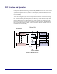
WN Hard DDR3 Controller WC Hard DDR3 Controller EC Hard DDR3 Controller EC IO Cluster ES IO Cluster EN IO Cluster EN Hard DDR3 Controller WN IO Cluster WC IO Cluster ES Hard DDR3 Controller WS Hard DDR3 Controller WS IO Cluster Core Fabric Figure 3: Speedster22iHD IO Cluster Organization The next sections will discuss the actual PHY implementation for the different memory interfaces in more detail.
DDR PHY Organization and Interfaces Figure 4 provides a block diagram view of how the DDR PHY is organized, and how it interfaces with other components of the memory interface sub-system. As shown, a PLL input clock and an external reset are supplied to the DDR PHY, which can communicate with 3 separate interfaces: an external DDR memory, and based on the user’s implementation, either the hard DDR controller in the IO ring or a soft DDR controller in the FPGA fabric.
Table 1: DDR PHY – Hard/Soft Controller Interface Port List Bus Signal Name Direction Description Width clk reset_n phy_ddr_clk_en byte_{3,2,1,0}_from_ctrl_{a,b} clk_div2 clk_div4 1 1 1 10 1 1 Input Input Input Input Output Output phy_ci_dq{a,b,c,d} N Input phy_ci_dq{a,b,c,d}8 N/8 Input phy_co_dq{a,b,c,d} N Output 1 1 9 9 9 9 9 9 9 N/8 1 9 9 9 1 1 9 9 1 Input Input Output Output Output Output Output Output Output Input Input Input Input Input Input Output Output Output Input User reference clo
Signal Name phy_ctrli_dq/dqs_croe{a,b} phy_ctrlo_write_level_out Signal Name Bus Width Direction N/8 N/8 Input Output Description Data a and b termination resistance enable signal for dq/dqs Write leveling output for byte Table 2: DDR PHY External Memory Interface Port List Bus Direction Description Width sd_clk_p sd_clk_n sd_cke sd_odt sd_ras_n sd_cas_n sd_we_n sd_reset_n sd_a sd_ba sd_cs_n sd_dm sd_dummy sd_dq sd_dqsn sd_dqsp 3 3 4 4 1 1 1 1 16 3 4 N/8 N/8 N N/8 N/8 Parameter DSIZE Output Outpu
PHY Structure and Operation Figure 5 below illustrates a high level overview of the DDR PHY structure. It consists of up to 9 data byte lanes, each implementing a x8 interface to give a max width of x72. There are also 4 byte lanes to implement Control, Address, Command (CAC) functions. Three of the CAC byte lanes operate at full rate mode and one of them operates in half-rate mode (denoted by the extension SD).
PHY – Controller Interfacing through Widebus The DDR PHY in Speedster22i HD devices provides a half-rate interface to the programmable logic fabric. Clearly, at high DDR3 data rates, running a soft controller and the application interface at half-rate speeds is impractical and often infeasible, as far as being able to close timing on the design. Typically, with design complexities and fabric limitations, the target core fmax should be no higher than 250MHz-300MHz.
Byte Lane Building Blocks As shown in Figure 5, the DDR PHY is made up of up to 9 data byte lanes (for a x72 mode interface) and 4 CAC (Control, Address and Command) byte lanes, 1 one of them operating at half rate, as denoted by the SD postfix. The building blocks inside these byte lanes are very similar. This section will detail the building blocks in a data byte lane and then explain the differences that can be seen in a CAC byte lane.
ddr3_dq9_bit/postamble/ddr3_dqs_bit: These are the modules used to transmit and receive dqs pulses to sample the data at dq. The chapter on DQS Clocking and Circuitry provides more detail about the functionality of each of these blocks and how the dqs is adjusted to ensure that the dq data is sampled optimally. The dqs output is provided to all of the dq and dm bits as a clock. It can also be routed as an output to the FPGA fabric. write leveling circuitry: There are 2 slave DLLs (sdlls), denoted as 0.
TX, RX and OE paths in Data Bits This section highlights the pieces of the TX, RX and OE circuitry that make up each of the data bits. These same pieces are also used in building clock, dqs and dm bits also, and the flexibility provided enables more custom IO configurations to be created as well. Figure 8 shows a block level diagram of the TX, RX and OE paths. The paths and the modules used are described in more detail below.
Transmit path: If half-rate (or quarter-rate with the widebus wrapper) is used in the fabric, four-wide data is provided from the fabric to a tx_sd module. The tx_sd module converts the incoming data from half-rate to full-rate and provides a two-wide data into the tx_any module (tx_sd module should be bypassed if a full-rate interface is used in the fabric).
DQS Clocking and Circuitry The circuitry in Figure 9 below shows how the DQS signal coming from or going to dqsn/dqsp is treated to ensure that both reads and writes can be successfully done for high data rate DDR3 implementations.
DLL Specs and Operation The DLL IP block in the Speedster22i HD1000 is wide range DLL with 1 Master DLL (MDLL) and 12 Slave DLLs (SDLLs). Table 5 provides the DLL IP Specs and Figure 10 provides a high-level block diagram of the DLL architecture.
The MDLL uses a regulated supply generated by a high performance on-board regulator to achieve the best possible performance in terms of jitter. It gets a clock as its reference to generate desired delay in its delay cells. The delay cells used in its VCDL is based on a current starved technique to provide the delay to generate the feedback signal. The phase of the feedback signal is compared with the reference signal.
Mux Output Option Ph0 Ph1 9 10 11 12 13 14 15 16 180 202.5 225 247.5 270 292.5 315 337.5 202.5 225 247.5 270 292.5 315 337.5 360 In the second stage the phase interpolator mixes the two phases (ph0 and ph1) mentioned above to meet the required delay/phase difference. For example, to push out the incoming signal by a 100 degree phase, the first stage selects phase 90 and phase 112.5, and then the second stage uses this pair and fine tunes it to meet the required 100 degree push out.
Revision History The following table shows the revision history for this document. 20 Date Version 04/26/2014 1.0 Revisions Initial Achronix release.