
Specifications

ADC12D1000RF, ADC12D1600RF
www.ti.com
SNAS519G –JULY 2011–REVISED APRIL 2013
To use this feature in ECM, use the Configuration Registers (Addr: 3h and Bh). See Input Control and
Adjust for more information.
6.2.1.10 AC/DC-Coupled Mode Pin (V
CMO
)
The V
CMO
Pin serves a dual purpose. When functioning as an output, it provides the optimal common-
mode voltage for the DC-coupled analog inputs. When functioning as an input, it selects whether the
device is AC-coupled (logic-low) or DC-coupled (floating). This pin is always active, in both ECM and Non-
ECM.
6.2.1.11 LVDS Output Common-mode Pin (V
BG
)
The V
BG
Pin serves a dual purpose. When functioning as an output, it provides the bandgap reference.
When functioning as an input, it selects whether the LVDS output common-mode voltage is higher (logic-
high) or lower (floating). The LVDS output common-mode voltage is specified as V
OS
and may be found in
Converter Electrical Characteristics Digital Control and Output Pin Characteristics. This pin is always
active, in both ECM and Non-ECM.
6.2.2 Extended Control Mode
In Extended Control Mode (ECM), most functions are controlled via the Serial Interface. In addition to this,
several of the control pins remain active. See Table 6-4 for details. ECM is selected by setting the ECE
Pin to logic-low. If the ECE Pin is set to logic-high (Non-ECM), then the registers are reset to their default
values. So, a simple way to reset the registers is by toggling the ECE pin. Four pins on the
ADC12D1600/1000RF control the Serial Interface: SCS, SCLK, SDI and SDO. This section covers the
Serial Interface. The Register Definitions are located at the end of the datasheet so that they are easy to
find, see Register Definitions.
6.2.2.1 The Serial Interface
The ADC12D1600/1000RF offers a Serial Interface that allows access to the sixteen control registers
within the device. The Serial Interface is a generic 4-wire (optionally 3-wire) synchronous interface that is
compatible with SPI type interfaces that are used on many micro-controllers and DSP controllers. Each
serial interface access cycle is exactly 24 bits long. A register-read or register-write can be accomplished
in one cycle. The signals are defined in such a way that the user can opt to simply join SDI and SDO
signals in his system to accomplish a single, bidirectional SDI/O signal. A summary of the pins for this
interface may be found in Table 6-2. See Figure 4-9 for the timing diagram and Converter Electrical
Characteristics Serial Port Interface for timing specification details. Control register contents are retained
when the device is put into power-down mode. If this feature is unused, the SCLK, SDI, and SCS pins
may be left floating because they each have an internal pull-up.
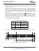
Table 6-2. Serial Interface Pins
Pin Name
C4 SCS (Serial Chip Select bar)
C5 SCLK (Serial Clock)
B4 SDI (Serial Data In)
A3 SDO (Serial Data Out)
SCS: Each assertion (logic-low) of this signal starts a new register access, i.e. the SDI command field
must be ready on the following SCLK rising edge. The user is required to de-assert this signal after the
24th clock. If the SCS is de-asserted before the 24th clock, no data read/write will occur. For a read
operation, if the SCS is asserted longer than 24 clocks, the SDO output will hold the D0 bit until SCS is
de-asserted. For a write operation, if the SCS is asserted longer than 24 clocks, data write will occur
normally through the SDI input upon the 24th clock. Setup and hold times, t
SCS
and t
HCS
, with respect to
the SCLK must be observed. SCS must be toggled in between register access cycles.
Copyright © 2011–2013, Texas Instruments Incorporated Functional Description 39
Submit Documentation Feedback
Product Folder Links: ADC12D1000RF ADC12D1600RF