
Specifications


ADC12D1000RF, ADC12D1600RF
SNAS519G –JULY 2011–REVISED APRIL 2013
www.ti.com
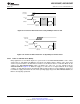
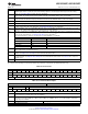
Table 6-13. Balun Recommendations
Balun Bandwidth
Mini Circuits TC1-1- 4.5 - 3000MHz
13MA+
Anaren 400 - 3000 MHz
B0430J50100A00
Mini Circuits ADTL2- 30 - 1800 MHz
18
6.5 Register Definitions
Eleven read/write registers provide several control and configuration options in the Extended Control
Mode. These registers have no effect when the device is in the Non-extended Control Mode. Each register
description below also shows the Power-On Reset (POR) state of each control bit. See Table 6-14 for a
summary.
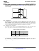
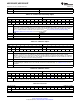
Table 6-14. Register Addresses
A3 A2 A1 A0 Hex Register Addressed
0 0 0 0 0h Configuration Register 1
0 0 0 1 1h Reserved
0 0 1 0 2h I-channel Offset Adjust
0 0 1 1 3h I-channel Full-Scale Range Adjust
0 1 0 0 4h Calibration Adjust
0 1 0 1 5h Calibration Values
0 1 1 0 6h Reserved
0 1 1 1 7h DES Timing Adjust
1 0 0 0 8h Reserved
1 0 0 1 9h Reserved
1 0 1 0 Ah Q-channel Offset Adjust
1 0 1 1 Bh Q-channel Full-Scale Range Adjust
1 1 0 0 Ch Aperture Delay Coarse Adjust
1 1 0 1 Dh Aperture Delay Fine Adjust
1 1 1 0 Eh AutoSync
1 1 1 1 Fh Reserved
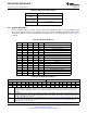
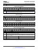
Table 6-15. Configuration Register 1
Addr: 0h (0000b) POR state: 2000h
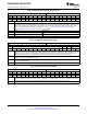
Bit 15 14 13 12 11 10 9 8 7 6 5 4 3 2 1 0
Name CAL DPS OVS TPM PDI PDQ Res LFS DES DEQ DIQ 2SC TSE SDR Res
POR 0 0 1 0 0 0 0 0 0 0 0 0 0 0 0 0
Bit 15 CAL: Calibration Enable. When this bit is set to 1b, an on-command calibration is initiated. This bit is not reset automatically
upon completion of the calibration. Therefore, the user must reset this bit to 0b and then set it to 1b again to execute another
calibration. This bit is logically OR'd with the CAL Pin; both bit and pin must be set to 0b before either is used to execute a
calibration.
Bit 14 DPS: DCLK Phase Select. In DDR, set this bit to 0b to select the 0° Mode DDR Data-to-DCLK phase relationship and to 1b to
select the 90° Mode. In SDR, set this bit to 0b to transition the data on the Rising edge of DCLK; set this bit to 1b to transition
the data on the Falling edge of DCLK.
(1)
Bit 13 OVS: Output Voltage Select. This bit sets the differential voltage level for the LVDS outputs including Data, OR, and DCLK. 0b
selects the lower level and 1b selects the higher level. See V
OD
in Converter Electrical Characteristics Digital Control and
Output Pin Characteristics for details.
(1) This pin / bit functionality is not tested in production test; performance is tested in the specified/default mode only.
64 Functional Description Copyright © 2011–2013, Texas Instruments Incorporated
Submit Documentation Feedback
Product Folder Links: ADC12D1000RF ADC12D1600RF