DIN EN ISO 9001:2008 certified ADDI-DATA GmbH Airpark Business Center Airport Boulevard B210 77836 Rheinmünster Germany Phone: +49 7229 1847–0 Fax: +49 7229 1847–222 E-mail: info@addi-data.com www.addi-data.com Technical description APCI-3010, APCI-3016, APCI-3110 and APCI-3116 Analog I/O board, optically isolated Edition: 02.
Product information This manual contains the technical installation and important instructions for correct commissioning and usage, as well as production information according to the current status before printing. The content of this manual and the technical product data may be changed without prior notice. ADDI-DATA GmbH reserves the right to make changes to the technical data and the materials included herein.
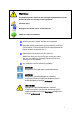
Warning! The following risks result from the improper implementation of the board and from use contrary to the regulations: Personal injury Damage to the board, the PC and peripherals Pollution of the environment. Protect yourself, others and the environment! Read the safety precautions (yellow leaflet) carefully! If this leaflet is not enclosed with the documentation, please contact us and ask for it.
Contents APCI-3xxx WARNING!...................................................................... 3 1 DEFINITION OF APPLICATION ............................... 7 1.1 Intended use ....................................................................7 1.2 Usage restrictions.............................................................7 1.3 Limits of use......................................................................7 1.4 General description of the board ....................................
Contents APCI-3xxx 7.3.3 7.3.4 Digital inputs (24 V) .............................................................. 25 Digital outputs (24 V)............................................................ 26 8 FUNCTIONS OF THE BOARD ................................ 27 8.1 Block diagram................................................................27 8.2 Analog inputs .................................................................27 8.2.1 8.2.2 8.2.3 8.2.4 Overview.................................
Contents APCI-3xxx Figures Fig. 3-1: Correct handling ................................................................ 11 Fig. 4-1: Required slots .................................................................... 13 Fig. 5-1: PCI slot types ...................................................................... 17 Fig. 5-2: Inserting the board ............................................................. 18 Fig. 5-3: Fastening the board at the back cover ............................. 18 Fig.
APCI-3xxx 1 Definition of application DEFINITION OF APPLICATION 1.1 Intended use The board APCI-3xxx 1 must be inserted in a PC with PCI slots which is used as electrical equipment for measurement, control and laboratory pursuant to the standard EN 61010-1 (IEC 61010-1). The used personal computer (PC) must fulfil the requirements of IEC 60950-1 or EN 60950-1 and EN 55022 or IEC/CISPR 22 and EN 55024 or IEC/CISPR 24.
Definition of application 1.4 APCI-3xxx General description of the board Characteristics The board has up to 16 single-ended input channels or up to 8 differential input channels for processing analog signals. Table 1-1: Overview Characteristics APCI-3010 APCI-3016 APCI-3110 APCI-3116 Analog inputs: Single-ended (SE) or differential (diff.
APCI-3xxx Definition of application The screw terminal panel PX 901-AG or the connection box PX-BNC allows the connection of the analog signals to the peripheral through the standard cable ST010. Through the screw terminal panel PX 8000 or PX8001, the standard cable ST 370-16 and the ribbon cable FB 8001 the digital signals are connected to the peripheral.
User 2 APCI-3xxx USER 2.1 Qualification Only persons trained in electronics are entitled to perform the following works: - installation - commissioning - use - maintenance 2.2 Country-specific regulations Consider the country-specific regulations about: - the prevention of accidents - electrical and mechanical installations - Electromagnetic compatibility (EMC).
APCI-3xxx 3 Handling of the board HANDLING OF THE BOARD Fig. 3-1: Correct handling Hold the board cautiously at the outer end and at the slot bracket.
Technical data 4 APCI-3xxx TECHNICAL DATA 4.1 Electromagnetic compatibility (EMC) The board APCI-3xxx is suited for installation in personal computers (PCs) which comply with the European EMC directive. The board APCI-3xxx complies with the European EMC directive. The tests were carried out by a certified EMC laboratory in accordance with the standard from the EN 61326 series (IEC 61326). The limit values as set out by the European EMC directive for an industrial environment are complied with.
APCI-3xxx Technical data Accessories 1 : For analog I/O: Cable: ........................................................ - ST010 Screw terminal panel: ................................ - PX 901-AG or connection box: ..................................... - PX-BNC For digital I/O: Cable: ........................................................ - FB 8001 - ST370-16 Screw terminal panel: ................................
Technical data APCI-3xxx 4.3.1 Analog inputs Number of channels: .................................. 16 analog inputs Resolution (APCI-3010 and APCI-3110): 12-bit Resolution (APCI-3016 and APCI-3116): 16-bit Max. throughput rate: ................................ 200 kHz (total sampling rate with all channels) Optical isolation: ........................................1000 V (1 second tested) Temperature drift: ......................................10 ppm/K Linearity error of the ADC:.......................
APCI-3xxx Technical data Logic input level: .......................................UH (max.): 30 V UH (min.): 19 V UL (max.): 14 V UL (min.): 0V Input frequency: .........................................1 MHz (max.) at 24 V Interruptible inputs:....................................Not available 4.3.4 Digital outputs (24 V Number of channels: ..................................4 digital outputs Optical isolation: ........................................1000 V (1 s tested) Output type:.......................
Technical data APCI-3xxx Logic output level: UH (typ.) ....................................................3.3 V at Iout = - 100 μA UH (min.) ...................................................2.4 V at Iout = -20 mA UL (max.)...................................................0.55 V at Iout = 20 mA 4.3.6 Timer, counter and watchdog Timer, interruptible: Number: ....................................................3 Timer depth: ..............................................16-bit Time base: ...............
APCI-3xxx 5 Installation of the board INSTALLATION OF THE BOARD Risk of injury! Please follow the safety precautions! An improper handling of the board may cause property damage and injury. 5.1 Opening the PC ♦ Switch off your PC and all the units connected to it. ♦ Pull the PC mains plug from the socket. ♦ Open your PC as described in the manual of the PC manufacturer. 5.2 Selecting a free slot ♦ Insert the board into a free PCI 5 V or PCI 3.3 V (32/64-bit) slot. Fig.
Installation of the board 5.3 APCI-3xxx Plugging the board into the slot ♦ Insert the board vertically into the chosen slot. Fig. 5-2: Inserting the board ♦ Fasten the board to the rear of the PC housing with the screw which was fixed on the back cover. Fig. 5-3: Fastening the board at the back cover ♦ Tighten all loose screws. 5.4 Closing the PC ♦ Close your PC as described in the manual of the PC manufacturer.
APCI-3xxx 6 Driver installation DRIVER INSTALLATION Information on how to select and download the appropriate driver can be found in the document “Quick installation PC boards” (see PDF link). The installation of drivers of the type “ADDI-DATA Multiarchitecture Device Drivers 32-/64-Bit for x86/AMD64” as well as the installation of the corresponding samples is described in the installation instructions (see PDF link). 6.
Connecting the peripherals 7 CONNECTING THE PERIPHERALS 7.1 Connector pin assignment Fig.
APCI-3xxx Connecting the peripherals Fig. 7-2: 50-pin connector (TTL I/O) NOTICE! The numbering of the 50-pin SUB-D connector corresponds to the usual numbering as printed on the connector for the LP mounting. However, on the connector for the connection to a ribbon cable a different numbering is printed as on the connector (corresponds to the numbering of the ribbon cable).
Connecting the peripherals APCI-3xxx Table 7-1: Connection of the digital inputs and outputs (24 V and TTL) FB8001 Board Pin No. (50-pin SUB-D male connector) Pin No.
APCI-3xxx Connecting the peripherals FB8001 Board Pin No. (50-pin SUB-D male connector) Pin No.
Connecting the peripherals APCI-3xxx Fig. 7-3: Connection of the screw terminal panel NOTICE! Plug the FB8001 cable into the connector of the board by inserting the red (or blue or black) cable line into pin 1. 7.3 Connection examples 7.3.1 Analog inputs Fig.
APCI-3xxx Connecting the peripherals 7.3.2 Analog outputs (only APCI-3110 and APCI-3116) Fig. 7-5: Connection example: Analog outputs 7.3.3 Digital inputs (24 V) Fig.
Connecting the peripherals 7.3.4 Digital outputs (24 V) Fig.
APCI-3xxx Functions of the board 8 FUNCTIONS OF THE BOARD 8.1 Block diagram Fig. 8-1: Block diagram: APCI-3010 and APCI-3016 Fig. 8-2: Block diagram: APCI-3110 and APCI-3116 8.2 Analog inputs There are 16 analog input channels on the boards – the resolution of the APCI-3010 and APCI-3110 is 12-bit and of the APCI-3016 and APCI-3116 16-bit.
Functions of the board APCI-3xxx 8.2.1 Overview Up to 16 analog Single Ended or up to 8 analog differential signals can be connected to the board. After the signals are transferred over a filter (RC-component) to a multiplexer (time multiplexed system), they are lead over a programmable instrumental gain to a 16-bit A/D converter (or 12-bit for APCI-3010 and APCI-3110). Data acquisition with the APCI-3xxx is based on a time-multiplex system.
APCI-3xxx Functions of the board Please note: During the switching of the voltage range from unipolar to bipolar or from bipolar to unipolar there is a longer settling time of the measuring chain. 8.2.3 Analog input switch (differential inputs) The input impedance is the input resistance (1012 Ω) of the PGA and the connected capacities (C1 and C2). Input impedance= 1012 Ω || 5 nF Fig. 8-3: Analog input switch (differential) *R Strom = optional component part for the version current.
Functions of the board 1) APCI-3xxx Simple mode The software initializes and starts the A/D conversion and after this step it reads the digital value of one or more channels.
APCI-3xxx Functions of the board b) Single hardware triggered scan This scan can be triggered with rising or falling edge (software initializes it).
Functions of the board APCI-3xxx d) Continuous software scan with timer delay e) Continuous hardware triggered scan Note: In this scan mode the external signal triggers only one scan at a time! f) Continuous hardware triggered scan with timer delay 32
APCI-3xxx 3) Functions of the board Sequence modes (with DMA) There are 2 sequence modes that are shown in the following two examples: a) Simple sequence mode (example 1 and 2) b) Sequence mode with delay (example 1 and 2) Note: The sequence mode always uses DMA! a) Simple sequence mode Simple sequence mode – Example 1 In this example the interrupt occurs at the end of each sequence (after 5 acquisitions) and the acquisition is stopped after 3 sequences.
Functions of the board APCI-3xxx dw_NbrOfChannel =5 dw_SequenceChannelArray = 0, 1, 2, 3, 4 b_DelayTimeMode = ADDIDATAG_DELAY_NOT_USED dw_SequenceCounter =0 dw_InterruptSequenceCounter= 2 b) Sequence mode with delay Sequence mode with delay - example 1 The interrupt occurs after the second sequence (10 acquisitions) and the acquisition is stopped. The total delay time from the start of one sequence to the next one is 100 µs.
APCI-3xxx Functions of the board dw_DelayTime = 20 dw_SequenceCounter = 2 dw_InterruptSequenceCounter= 2 4) Auto refresh mode The analog acquisition is initialized and writes the values of the channels into a storage location on the APCI-3xxx. The PC reads the data asynchronous to the acquisition. 8.3 Analog outputs There are 4 analog output channels with a resolution of 12-bit and a precision of 11-bit on the APCI-3110 and APCI-3116.
Functions of the board APCI-3xxx Fig. 8-4: Reaction time of the analog outputs When the computer is switched on, the analog outputs are temporarily in an undefined state. It is thus essential that the computer is switched on before the connected peripherals. After the Power ON reset of the computer, a voltage of 0 V is applied to all analog outputs. Fig.
APCI-3xxx 8.4 Functions of the board Digital inputs The inputs are designed for the acquisition of external signal states: The input information is loaded as numerical value into a memory unit of the PC by software. This numeric value calculates the state of the inputs signals. 24 V optically isolated inputs They correspond to the 24 V industrial standard (IEC1131-2): - logic"1" corresponds to an input voltage superior to 19 V - logic"0" corresponds to an input voltage inferior to 14V.
Functions of the board 8.5 APCI-3xxx Digital outputs The APCI-3xxx has 4 optically isolated outputs. The positive logic is applied: - logic"1": Sets the output by software. - logic"0": Resets the output. NOTICE! The supply unit for the external voltage supply of the board must supply the power that is needed for your application. The max. supply voltage is 35 V. For each output a current of 50 mA can be set.
APCI-3xxx 8.6 Functions of the board TTL inputs and outputs The board APCI-3xxx has 24 TTL channels that are divided into three ports: Table 8-1: TTL I/O (ports) Port Description Channel Port 0 Output Channel 0-7 Port 1 Input Channel 8-15 Port 2 Programmable I/O Channel 16-23 Fig. 8-8: Block diagram of the TTL I/O 8.7 Watchdog A 16-bit watchdog is available for the analog outputs and for the 24 V outputs. After its reload value (timeout) the watchdog resets the outputs.
Functions of the board 8.8 APCI-3xxx Timer The 16-bit timer is a downwards counter that can generate an interrupt after the reload value (timeout). With the timer a time base is provided independent from the PC clock, with which for example operations can be synchronized. The status of the counter value and of the reload value as well as the status and interrupt register can be read back through software. The operation states can be read back.
APCI-3xxx Functions of the board Upward counter Fig. 8-9: Run down of the upward counter After reaching the reload value, the counting value is set on 0 and continues to be counted. At an overflow an interrupt can be generated. Downward counter Fig. 8-10: Run down of the downward counter In order to get the same counting value as in the upwards mode, the reload value must be set on 3. The counter counts down to 0 and will be reset to the reload value from the next edge cycle on.
Functions of the board APCI-3xxx 8.10 Setting a digital output At the run down of the counter/timer/watchdog a digital output (24 V) can be set. Here also the output level can be defined. The output will be enabled for an (input) clock. Fig.
APCI-3xxx 9 Standard software STANDARD SOFTWARE The API software functions supported by the board are listed in an HTML document. A description on how to access the respective file can be found in the document “Quick installation PC boards” (see PDF link), in the chapter “Standard software”.
Return or disposal 10 APCI-3xxx RETURN OR DISPOSAL 10.1 Return If you need to return your board, you should read the following checklist before. Checklist for returning the board: • Specify the reason for returning your board (e.g. exchange, modification, repair), the serial number of the board, the contact person in your company including his/her telephone extension and e-mail address, as well as the mailing address for a potential new delivery. You do not have to indicate the RMA number. Fig.
APCI-3xxx Return or disposal 10.2 Disposal of ADDI-DATA waste equipment ADDI-DATA organises the disposal of ADDI-DATA products that were put on the German market after 13 August 2005. If you want to return waste equipment, please e-mail your request to: rohs@addi-data.com. Boards that were delivered after 13 August 2005 can be recognised by the following label: Fig. 10-2: Disposal: Label This symbol indicates the disposal of waste electrical and electronic equipment.
Appendix 11 APCI-3xxx APPENDIX 11.1 Glossary Table 11-1: Glossary Term A/D converter Acquisition Analog Auto refresh mode Clock D/A converter Data acquisition DC voltage Differential inputs (DIFF) Disturb signal Driver Edge FIFO 46 Description = ADC An electronic device that produces a digital output directly proportional to an analog signal output. The process by which data is gathered by the computer for analysis or storage.
APCI-3xxx Appendix Term Gain Ground Impedance Inductive loads Input impedance Input level Interrupt Level Limit value MUX Noise immunity Noise suppression Operating voltage Description The factor by which an incoming signal is multiplied. A common reference point for an electrical system. The reciprocal of admittance. Admittance is the complex ratio of the voltage across divided by the current flowing through a device, circuit element, or network. The voltage over the inductor is U=L.
Appendix APCI-3xxx Term Optical isolation Output voltage Parameter PCI bus Protective circuitry Protective diode Reference voltage Reference voltage Resolution Scan mode Sensor Sequence mode Settling time Short circuit Short circuit current 48 Description The technique of using an optoelectric transmitter and receiver to transfer data without electrical continuity, to eliminate high-potential differences and transients.
APCI-3xxx Appendix Term Signal delay Simple mode Single Ended inputs (SE) Synchronous Throughput rate Timer Trigger TTL Description The change of a signal affects the following circuitries with finite velocity; the signal will be delayed. Besides the signal delay times that are not wanted, the signal delay can be extended by time switches and delay lines. The software initializes and starts the A/D conversion and after this step it reads the digital value of one or more channels.
Appendix APCI-3xxx 11.