NuDAQ PCI-9111DG/HR Multi-Functions Data Acquisition Card User’s Guide
@Copyright 1997~2000 ADLINK Technology Inc. All Rights Reserved. Manual Rev 2.21: September 7, 2000 The information in this document is subject to change without prior notice in order to improve reliability, design and function and does not represent a commitment on the part of the manufacturer.
Getting service from ADLINK ♦ Customer Satisfaction is always the most important thing for ADLINK Tech Inc. If you need any help or service, please contact us and get it. ADLINK Technology Inc. http://www.adlink.com.tw Web Site http://www.adlinktechnology.com Sales & Service service@adlink.com.tw NuDAQ nudaq@adlink.com.tw NuDAM nudam@adlink.com.tw Technical NuIPC nuipc@adlink.com.tw Support NuPRO nupro@adlink.com.tw Software sw@adlink.com.tw TEL +886-2-82265877 FAX +886-2-82265717 Address 9F, No.
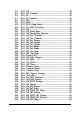
Table of Contents How to Use This Guide ............................................v Chatper 1 Introduction .......................................... 1 1.1 1.2 1.3 1.4 Features.......................................................................... 1 Applications.................................................................... 2 Specifications ................................................................. 2 Software Supporting....................................................... 4 1.4.1 1.4.
3.3 3.4 3.5 3.6 3.7 3.8 3.9 3.10 3.11 3.12 3.13 3.14 3.15 3.16 A/D Data Registers........................................................ 14 A/D Channel Control Register....................................... 15 A/D Channel Read Back Register.................................. 16 A/D Input Signal Range Control Register...................... 16 A/D Range and Status Readback Register.................... 17 A/D Trigger Mode Control Register............................... 17 Software Trigger Register...........
5.4 5.5 5.6 5.7 5.8 5.9 5.10 5.11 5.12 5.13 5.14 5.15 5.16 5.17 5.18 5.19 5.20 5.21 5.22 5.23 5.24 5.25 5.26 5.27 5.28 5.29 5.30 5.31 5.32 5.33 5.34 5.35 5.36 5.37 5.38 5.39 5.40 5.41 5.42 5.43 5.44 _9111_DO ..................................................................... 38 _9111_DO_Channel ...................................................... 39 _9111_DI ....................................................................... 39 _9111_DI_Channel ......................................................
Chatper 6 Calibration........................................... 65 6.1 6.2 6.3 6.4 What do you need......................................................... 65 VR Assignment ............................................................. 66 A/D Adjustment............................................................. 66 D/A Adjustment............................................................. 67 6.4.1 6.4.2 Unipolar Analog Output ...........................................................
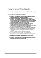
How to Use This Guide This manual is designed to help you to use the PCI-9111. The manual describes the versatile functions and the operation theorem of the PCI-9111 card. It is divided into six chapters: • • • • • • • Chapter 1, "Introduction", gives an overview of the product features, applications, and specifications. Chapter 2, "Installation", describes how to install the PCI-9111.
1 Introduction The PCI-9111 is an advanced data acquisition card based on the 32-bit PCI Bus architecture. High performance designs and the state-of-the-art technology make this card ideal for data logging and signal analysis applications in medical, process control, and etc. 1.
• • • • 1.2 Applications • • • • • • • • • • 1.3 Pre-trigger Control Integral DC-to-DC converter for stable analog power source 37-pin D-type connector Compact size: half-size PCB Industrial and laboratory ON/OFF control Energy management Communication 16 TTL/DTL compatible digital input channels Security controller Product test Period and pulse width measurement Event and frequency counting Waveform and pulse generation BCD interface driver Specifications ♦ Analog Input (A/D) • Converter: B.B.
♦ ♦ ♦ ♦ Unipolar: 0~10V Bipolar: -10V~+10V • Converter: DAC7541 or equivalent, monolithic multiplying • Settling Time: 30 µ sec • Linearity: ± 1/2 bit LSB • Output driving capability: ± 5mA max. Digital I/O (DIO) • Numbers of Channel: 16 TTL compatible inputs and outputs • Input Voltage: Low: Min. 0V; Max. 0.8V High: Min. +2.0V; Max. 5.5V • Input Load: Low: +0.8V @ -0.2mA max. High: +2.7V @ +20mA max. • Output Voltage: Low: Min. 0V; Max. 0.4V High: Min. +2.4V; Max. 5.5V • Driving Capacity: Low: Max. +0.
• • • • • 1.4 Operating Temperature: 0° C ~ 60° C Storage Temperature: -20° C ~ 80° C Humidity: 5 ~ 95%, non-condensing Power Consumption: +5 V @ 570 mA typical Dimension: Compact size only 172mm x 105mm Software Supporting ADLink provides versatile software drivers and packages for users’ different approach to built-up a system.
The above software drivers are shipped with the board. Please refer to the “Software Installation Guide” to install these drivers. 1.4.2 ® PCIS-LVIEW: LabVIEW Driver PCIS-LVIEW contains the VIs, which are used to interface with NI’s ® LabVIEW software package. The PCIS-LVIEW supports Windows ® 95/98/NT/2000. The LabVIEW drivers are free shipped with the board. You can install and use them without license. For detail information about PCIS-LVIEW, please refer to the user’s guide in the CD.
target drivers o f r ISaGRAF under Windows NT environment. PCIS-ISG is included in the ADLINK CD. It needs license. 1.4.8 TM PCIS-ICL: InControl The Driver PCIS-ICL is the InControl driver which support the Windows NT. The PCIS-ICL is included in the ADLINK CD. It needs license. 1.4.9 PCIS-OPC: OPC Server PCIS-OPC is an OPC Server, which can link with the OPC clients. There are many software packages on the market can provide the OPC clients now. The PCIS-OPC supports the Windows NT.
2 Installation This chapter describes how to install the PCI-9111. At first, the contents in the package and unpacking information that you should be careful are described. The PCI-9111 does an automatic configuration of the IRQ, port address, and BIOS address. Therefore, it is not necessary to set the above configurations as you use ISA DAS card. 2.
Inspect the card module carton for obvious damage. Shipping and handling may cause damage to your module. Be sure there are no shipping and handing damages on the module before processing. After opening the card module carton, extract the system module and place it only on a grounded anti-static surface component side up. Again inspect the module for damage. Press down on all the socketed IC's to make sure that they are properly seated. Do this only with the module place on a firm flat surface.
2.4 Jumper Descriptions The only one jumper (JP1) on the PCI-9111 card is used to set the range of the analog output channel. The analog output range could be unipolar (0~10V) or bi-polar (-10V~+10V). The default setting is bi-polar. BI Analog output range is JP1 -1 0 V ~ + 1 0 V BI Analog output range is JP1 0V~ +10V UI UI Figure 2.2 Analog output range setting 2.
5. Select a 32-bit PCI slot. PCI slots are shorter than ISA or EISA slots, and are usually white or ivory. 6. Before handling the PCI cards, discharge any static buildup on your body by touching the metal case of the computer. Hold the edge and do not touch the components. 7. Position the board into the PCI slot you selected. 8. Secure the card in place at the rear panel of the system. 2.
• CN 2: Digital Signal Output (DO 0 ~ 15) CN2 +12V GND DO 15 DO 13 DO 11 DO 9 DO 7 DO 5 DO 3 DO 1 20 18 16 14 12 10 8 6 4 2 19 17 15 13 11 9 7 5 3 1 +5V GND DO 14 DO 12 DO 10 DO 8 DO 6 DO 4 DO 2 DO 0 Figure 2.4 Pin Assignment of CN2 Legend: DO n DI n GND • : Digital output signal channel n : Digital input signal channel n : Digital ground CN 3: Analog Input/Output, Extended I/O, Trigger Signals CN3 N/C EDO2 EDO0 EDI3 EDI2 EDI1 EDI0 DA Out A.GND A.
EDO n A.GND D.GND N.C 2.8 : Extended Digital Output Channel n (0~3) : Analog Signal Ground : Digital Signal Ground : No connection Daughter Board Connection The PCI-9111 can be connected with five different daughter boards, ACLD-8125, ACLD-9137, 9138, 9182, 9185, and 9188. The functionality and connections are specified as follows. 2.8.1 Connect with ACLD-8125 The ACLD-8125 has a 37-pin D-sub connector, which can connect with PCI-9111 through 37-pin assemble cable.
3 Registers Format The detailed descriptions of the registers format are specified in this chapter. This information is quite useful for the programmers who wish to handle the card by low-level programming. However, we suggest users have to understand more about the PCI interface then start any low-level programming. In addition, the contents of this chapter can help users understand how to use software driver to manipulate this card. 3.
Please do not try to modify the base address and interrupt which assigned by the PCI PnP BIOS, it may cause resource confliction in your system. 3.2 I/O Address Map Most of the PCI-9111 registers are 16 bits. The users can access these registers by 16 bits I/O instructions. The following table shows the registers map, including descriptions and their offset addresses relative to the base address.
Address: BASE + 0h Attribute: read only Data Format: for 12-bits PCI-9111DG Bit 7 6 BASE+0h AD3 AD2 BASE+1h AD11 AD10 for 16-bits PCI-9111HR Bit 7 6 BASE+0h BASE+1h AD7 AD15 AD6 AD14 5 4 3 2 1 0 AD1 AD9 AD0 AD8 CH3 AD7 CH2 AD6 CH1 AD5 CH0 AD4 5 4 3 2 1 0 AD5 AD13 AD4 AD12 AD3 AD11 AD2 AD10 AD1 AD9 AD0 AD8 AD15 ~ AD0: Analog to digital data. AD11 is the Most Significant Bit (MSB) of PCI-9111DG while AD15 is the MSB of PCI-9111HR. AD0 is the Least Significant Bit (LSB).
3.5 A/D Channel Read Back Register The AD channel setting can be read back from this register. Address: BASE + 6h Attribute: read only Data Format: Bit 7 6 5 4 3 2 1 0 BASE+6h AS3 AS2 AS1 AS0 CN3 CN2 CN1 CN0 BASE+7h --------Where: CNn: channel number ASn: Auto scan channel number. There are 8 bits in this register. Under non-auto scan mode, the 4 LSBs (CN0~CN3) show the channel number setting and the 4 MSBs (AS3~AS0) is all ‘0’. Under auto-scan mode, the 4LSBs record the ending channel number.
3.7 A/D Range and Status Read back Register The A/D range setting and A/D FIFO status can be read back from this register.
ASCAN: Auto Scan Control 0: Auto Scan OFF 1: Auto Scan ON Only the modes listed below can be applied on the PCI-9111 card: Bit 3 Bit 2 Bit 1 Bit 0 Mode Description PTRG EITS TPST ASCAN 0/1 0 0 0/1 Software Trigger & Polling 0/1 0 1 0/1 Timer Pacer Trigger 0/1 1 X 0/1 External Trigger Note: 3.9 The bits in this register can only control the A/D trigger source and trigger method. The trigger conditions are independent from data transfer method and interrupt generation.
ISC1: FFEN: 3.
3.13 Extended I/O Ports The PCI-9111 provides four extended input signals and four extended output signals. The signals are on the 37 pin connector. The extended output signals can be read back from the high nibble (4 MSBs) of the extended input port. Note that the output EDO pins on CN3 (37 pin connector) can be set as one of the following mode by software. The definition of the setting value can be found in header file of the library ACL_PCI.H. 1. EDO_INPUT EDO mode 1 2. EDO_OUT_EDO EDO mode 2 3.
Bit 7 6 5 4 3 2 1 0 DI5 DI13 DI4 DI12 DI3 DI11 DI2 DI10 DI1 DI9 DI0 DI8 5 4 3 2 1 0 DO5 DO13 DO4 DO12 DO3 DO11 DO2 DO10 DO1 DO9 DO0 DO8 Base + 2h DI7 DI6 Base + 3h DI15 DI14 Address: BASE + 2h Attribute: write only Data Format: Bit 7 6 Base + 2h Base + 3h 3.15 DO7 DO15 DO6 DO14 D/A Output Register The D/A converter will convert the D/A output digital data to analog signal.
4 Operation Theorem The operation theorem of the functions on PCI-9111 card is described in this chapter. The functions include the A/D conversion, D/A conversion, Digital I/O and counter / timer. The operation theorem can help you to understand how to manipulate or to program the PCI-9111. 4.
4.1.1 A/D Conversion Procedure For using the A/D converter, users must know about the property of the signal to be measured at first. The users can decide which channels to be used and connect the signals to the PCI-9111. Refer to section 2.7 ‘Connectors Pin Assignment’. In addition, users should define and control the A/D signal sources, including the A/D channel, A/D gain, and A/D signal types. Please refer to section 4.1.2. For A/D signal source control.
Analog Input Signal Connection The PCI-9111 provides 16 single-ended analog input channels. The analog signal can be converted to digital value by the A/D converter. To avoid ground loops and get more accurate measurement of A/D value, it is quite important to understand the signal source type. The single-ended mode has only one input relative to ground and is suitable for connecting with the floating signal source. The floating source means it does not have any connection to real ground.
Signal Range The proper signal range is important for data acquisition. The input signal may be saturated if the A/D gain is too large. Sometimes, the resolution may be not enough if the signal is small. The maximum A/D signal range of PCI-9111 is +/- 10 volts when the A/D gain value is 1. The A/D gain control register controls the maximum signal input range. The signal gain is programmable with 5 levels (1, 2, 4, 8, 16).
refer to section 4.6 for timer/counter operation. This mode is ideal for high speed A/D conversion. It can be combined with the FIFO half full interrupt or EOC interrupt to transfer data. It is also possible to use software FIFO polling to transfer data. The A/D trigger, A/D data transfer and Interrupt can be set independently, most of the complex applications can thus be covered. It's recommend to use this mode if your applications need a fixed and precise A/D sampling rate.
It is possible to read A/D converted data without polling. The A/D conversion time will not exceed 8.5µs on PCI-9111 card. Hence, after software trigger, the software can wait for a t least 8.5µs then read the A/D register without polling. The data polling transferring is very suitable for the application need to process AD data in real time.
EOC Interrupt Transfer The PCI-9111 provides traditional hardware end-of-conversion (EOC) interrupt capability. Under this mode, an interrupt signal is generated when the A/D conversion is ended and the data is ready to be read in the FIFO. It is useful to combine the EOC interrupt transfer with the timer pacer trigger mode. After A/D conversion is completed, the hardware interrupt will be inserted and its corresponding ISR (Interrupt Service Routine) will be invoked and executed.
software must continuously read data out from the FIFO to prevent FIFO full. The software also should poll the counter value to check if the A/D sampling is stopped. To set up the Pre-Trigger mode, the following steps should be followed: 1. Set Pre-Trigger Mode Off: PTRG = OFF. 2. Set 8254 Counter #0 value N (N=1~65535). Note that the larger the counter value, the more host memory buffer is needed. 3. Set up A/D data acquire, including, A/D range, channel scan, data transfer mode and so on. 4.
4.1.6 A/D Data Format The A/D data read from the FIFO is in the two‘s complement format. As the A/D gain is 1, the A/D signal range is roughly +10V ~ -10V bi-polar. In PCI-9111HR, the whole 16 bits A/D data are available. The relationship between voltage and the A/D data value is shown in the following table: A/D Data (Hex) 7FFF 4000 0001 0000 FFFF C000 8001 8000 Note: Decimal Value +32767 +16384 1 0 -1 -16384 -32767 -32768 Voltage (Volts) +9.99969 +5.00000 +0.00031 0.00000 -0.00031 -5.00000 -9.
4.2 Interrupt Control 4.2.1 System Architecture The PCI-9111‘s interrupt system is a powerful and flexible system which is suitable for A/D data acquisition and many applications. The system is a Dual Interrupt System. The dual interrupt means the hardware can generate two interrupt request signals in the same time and the software can service these two request signals by ISR. Note that the dual interrupt does not mean the card occupies two IRQ levels.
users must check if another IRQ is also asserted, then clear current IRQ to allow the next IRQ occurring. The two IRQs are named as INT1 and INT2. INT1 comes from AD EOC or the FIFO half-full flag. INT2 comes from timer‘s pacer output or the external interrupt request. The sources of INT1 and INT2 are selective by the Interrupt Control (ISC) Register.
4.4 D/A Conversion The PCI-9111 has one analog output channel. The signal range can be uni-polar or bi-polar which are set by JP1. -10V Ref In Pin- 30 (DA Out) D/A Converter + To D/A Output Analog GND The operation of D/A conversion is simpler than A/D operation. You only need to write digital values into the D/A data registers and the corresponding voltage will be output from the DA Out (pin-30 of CN3). Refer to section 3.15 for information about the D/A data registers.
4.5 Digital Input and Output To program digital I/O operation is fairly straightforward. The digital input operation is just to read data from the corresponding registers, and the digital output operation is to write data to the corresponding registers. The digital I/O registers‘ format is shown in section 3.14. Note that the DIO data channel can only be read or written in form of 16 bits together. It is impossible to access individual bit channel.
4.6.2 Pacer Trigger Source The timer #1 and timer #2 are cascaded together to generate the timer pacer trigger of A/D conversion. The frequency of the pacer trigger is software controllable. The maximum pacer signal rate is 2MHz/4=500K which excess the maximum A/D conversion rate of the PCI-9111. The minimum signal rate is 2MHz/65535/65535, which is a very slow frequency that user may never use it.
5 C/C++ Library This chapter describes the software library for operating this card. Only the functions in DOS library and Windows 95 DLL are described. Please refer to the PCIS-DASK function reference manual, which included in ADLINK CD, for the descriptions of the Windows 98/NT/2000 DLL functions. The function prototypes and some useful constants are defined in the header files LIB directory (DOS) and INCLUDE directory (Windows 95). For Windows 95 DLL, the developing environment can be Visual Basic 4.
5.2 Programming Guide 5.2.1 Naming Convention The functions of the NuDAQ PCI cards or NuIPC CompactPCI cards’ software driver are using full-names to represent the functions' real meaning. The naming convention rules are: In DOS Environment: _{hardware_model}_{action_name}. e.g. _9111_Initial(). All functions in PCI-9111 driver are with 9111 as {hardware_model}. But they can be used by PCI-9111DG, PCI-9111HR.
5.3 _9111_Initial @ Description This function is used to initialize PCI_9111. Every PCI_9111 card has to be initialized by this function before calling other functions.
5.5 _9111_DO_Channel @ Description This function is used to write data to digital output ports. There are 16 digital output channels on PCI_9111. You can control each digital output channel by this function directly. When performing this function, the digital output port is written and the output status will be changed to the value you had specified to do_data.
cardNo: DIData: The card number of PCI-9111 card initialized The value accessed from digital input port @ Return Code ERR_NoError 5.7 _9111_DI_Channel @ Description This function is used to read data from digital input port. There are 16 digital input channels on PCI_9111. You can read each digital input channel by this function directly. As this function is performing, the digital input port is read and the value of the specified channel is stored in *data.
Visual Basic (Windows 95) W_9111_EDI (ByVal cardNo As Integer, DIData As Integer) As Integer @ Argument cardNo: The card number of PCI-9111 card initialized DIData: The value accessed from extended digital input port @ Return Code ERR_NoError 5.9 _9111_EDO @ Description There are 4 extended digital output channels on PCI_9111. This function is used to write data to extended digital output port. The extended digital output channels can be set as three modes (refer to section 6.2.
U16 _9111_EDO_Read_Back (U16 cardNo, U16 *DOData ) C/C++ (Windows 95) U16 W_9111_EDO_Read_Back (U16 cardNo, U16 *DOData ) Visual Basic (Windows 95) W_9111_EDO_Read_Back (ByVal cardNo As Integer, DOData As Integer) As Integer @ Argument cardNo: DOData: The card number of PCI-9111 card initialized The read back value @ Return Code ERR_NoError 5.
5.12 _9111_DA @ Description This function is used to write data to D/A converters. There are one Digital-to-Analog conversion channel on the PCI-9111. The resolution of each channel is 12 bit; i.e. the range is from 0 to 4095.
5.14 _9111_AD_Read_Data_Repeat @ Description This function is used to read the AD conversion data n times continuously.
ADChannelNo: selected channel number or the ending channel number to perform A/D conversion. @ Return Code ERR_NoError 5.16 _9111_AD_Get_Channel @ Description This function reads from the multiplexer scan channel register to get the AD channel number and the value is stored in ADChannelNo. Under non-auto scan mode, the bit 0 to 3 of ADChannelNo stores the channel number setting and the bit 4 to 7 of ADChannel is all ‘0”.
5.17 _9111_AD_Set_Range @ Description This function is used to set the A/D range by means of writing data to the gain control register. The initial value of gain is '1' which is the default setting by the PCI-9111 hardware. The relationship between gain and input voltage ranges in the following table: Input Range (V) ±10 V ±5 V ±2.5 V ±1.25 V ±0.
5.18 _9111_AD_Get_Range @ Description This function is used to get the A/D range from the gain control register. The relationship between gains and input voltage ranges are specified by following table. Input Range (V) ±10 V ±5 V ±2.5 V ±1.25 V ±0.
@ Argument cardNo: The card number of PCI-9111 card initialized ADStatus: The status of AD FIFO. The AD FIFO status could be one of the following: ADSTS_FF_EF: FIFO is empty ADSTS_FF_HF: FIFO is half-full ADSTS_FF_FF: FIFO is full, A/D data may have been loss ADSTS_BUSY: AD is busy, A/D data is written into FIFO. @ Return Code ERR_NoError 5.20 _9111_AD_Set_Mode @ Description This function is used to set AD trigger and channel scan mode. Please refer to section 5.1.
5.21 _9111_AD_Get_Mode @ Description This function is used to get AD mode. Please refer to section 5.1.3 for the detailed description of AD trigger modes and section 5.1.5 for the description of Pre-Trigger mode control.
W_9111_INT_Set_Reg (ByVal cardNo As Integer, ByVal INTC As Integer) As Integer @ Argument cardNo: INTC: The card number of PCI-9111 card initialized The value written to the interrupt control register @ Return Code ERR_NoError 5.23 _9111_INT_Get_Reg @ Description This function is used to get the AD mode setting and interrupt control setting by reading data from A/D mode and interrupt control read back register. The returned settings are stored in INTC. Please refer to section 4.7 and section 4.
Visual Basic (Windows 95) W_9111_Reset_FIFO (ByVal cardNo As Integer) As Integer @ Argument cardNo: The card number of PCI-9111 card initialized. @ Return Code ERR_NoError 5.25 _9111_AD_Soft_Trigger @ Description This function is used to trigger the A/D conversion by software. When the function is called, a trigger pulse will be generated and the converted data will be stored from address Base +0.
count: value to write, only 8 LSBs are effective @ Return Code ERR_NoError 5.27 _9111_Get_8254 @ Description This function is used to read PCI-9111 8254 Programmable Timer. The read value are stored in count.
W_9111_AD_Timer (ByVal cardNo As Integer, ByVal c1 As Integer, ByVal c2 As Integer) As Integer @ Argument cardNo: The card number of PCI-9111 card initialized. c1: frequency divider of timer #1 c2: frequency divider of timer #2 @ Return Code ERR_NoError 5.29 _9111_Counter_Start @ Description The counter #0 of the PCI-9111 Timer/Counter chip can be freely programmed by the users. This function is used to program the counter #0. This counter is used as the pre-trigger counter.
C/C++ (DOS) U16 _9111_Counter_Read (U16 cardNo, U16 *c0) C/C++ (Windows 95) U16 W_9111_Counter_Read (U16 cardNo, U16 *c0) Visual Basic (Windows 95) W_9111_Counter_Read (ByVal cardNo As Integer, c0 As Integer) As Integer @ Argument cardNo: The card number of PCI-9111 card initialized. c0: count value of counter#0 @ Return Code ERR_NoError 5.31 _9111_Counter_Stop @ Description This function is used to stop the timer operation. The timer is set as the “One-shot” mode with count value ‘0’.
5.32 _9111_INT_Source_Control @ Description The PCI-9111 has dual interrupts system, two interrupt sources can be generated and be checked by the software. This function is used to select and control PCI-9111 interrupt sources by writing data to interrupt control register. Please refer to section 5.2 for detailed description of interrupt system.
5.33 _9111_CLR_IRQ @ Description This function is used to clear interrupt request which is requested by PCI-9111. If you use EOC interrupt or FIFO half full interrupt to transfer A/D converted data, you should use this function to clear interrupt request status; otherwise, the new coming interrupt will not be generated.
5.35 _9111_Get_IRQ_Status @ Description This function is used to get the status of the two IRQs (INT1 and INT2) in PCI-9111 card. @ Syntax C/C++ (DOS) void _9111_Get_IRQ_Status (U16 cardNo, U16 *ch1, U16 *ch2) C/C++ (Windows 95) void W_9111_Get_IRQ_Status (U16 cardNo, U16 *ch1, U16 *ch2) Visual Basic (Windows 95) W_9111_Get_IRQ_Status (ByVal cardNo As Integer, ch1 As Integer, ch2 As Integer) @ Argument cardNo: ch1: ch2: the card number of PCI-9111 card initialized.
cardNo: ad_data: the card number of PCI-9111 card initialized. the 16bits A/D converted value. The data format can be referred to section 5.1.6 for details. @ Return Code ERR_NoError ERR_FIFO_Half_NotReady 5.37 _9111_AD_Aquire @ Description This function is used to trigger the A/D conversion data for PCI-9111 by software trigger. It reads the 12 bits A/D data when the data is ready.
W_9111_AD_HR_Aquire (ByVal cardNo As Integer, ad_data As Integer) As Integer @ Argument cardNo: ad_data: the card number of PCI-9111 card initialized. the 16bits A/D converted value. The data format can be referred to section 5.1.6 for details. @ Return Code ERR_NoError ERR_AD_AquireTimeOut 5.39 _9111_AD_INT_Start @ Description This function is used to initialize and start up the AD EOC (end-of-conversion) interrupt transfer mode.
Visual Basic (Windows 95) W_9111_AD_INT_Start (ByVal cardNo As Integer, ByVal auto_scan As Integer, ByVal ad_ch_no As Integer, ByVal ad_gain As Integer, ByVal count As Integer, ad_buffer As Integer, ByVal c1 As Integer, ByVal c2 As Integer) As Integer @ Argument cardNo: the card number of PCI-9111 card initialized. auto_scan: 0: autoscan is disabled. 1: autoscan is enabled. ad_ch_no: A/D channel number. If the auto_scan is set as enable, the selection sequence of A/D channel is: 0, 1, 2, 3, ...
function _9111_AD_FFHF_INT_Status(). While all the specified blocks of data are acquired, the interrupt status will be changed to “AD_FFHF_BLOCK_FULL”. The function can perform on single A/D channel (autoscan is disable) or multiple A/D channels (autoscan is enable) with fixed analog input range.
5.41 _9111_AD_INT_Status @ Description This function is used to check the status of interrupt operation. The _9111_AD_INT_Start() is executed on background, therefore you can issue this function to check the status of interrupt operation. While all the specified counts of data are acquired, the interrupt status will be changed to “AD_INT_STOP”.
C/C++ (Windows 95) U16 W_9111_AD_FFHF_INT_Status (U16 cardNo, U16 *status, U16 *blockNo) Visual Basic (Windows 95) W_9111_AD_FFHF_INT_Status (ByVal cardNo As Integer, status As Integer, blockNo As Integer) As Integer @ Argument cardNo: status: the card number of PCI-9111 card initialized. the status of the INT data transfer. The valid status code are the following: AD_FFHF_INT_RUN AD_FFHF_BLOCK_FULL the A/D conversion block number performed currently blockNo: @ Return Code ERR_NoError 5.
5.44 _9111_AD_INT_Stop @ Description This function is used to stop both the interrupt data transfer functions. After executing this function, the internal AD trigger is disabled and the AD timer is stopped. This function returns the number/block of data has been transferred, no matter whether the AD interrupt data transfer is stopped by this function.
6 Calibration In data acquisition process, how to calibrate the measurement devices to maintain its accuracy is very important. Users can calibrate the analog input and analog output channels under the users' operating environment for optimizing the accuracy. This chapter will guide you to calibrate your PCI-9111 to an accuracy condition. 6.
6.2 VR Assignment There are five variable resistors (VR) on the PCI-9111 board to allow you making accurate adjustment on A/D and D/A channels. The function of each VR is specified as Table 6.1. VR1 VR2 VR3 VR4 VR5 D/A full scale adjustment D/A offset adjustment A/D offset adjustment A/D full scale adjustment A/D programmable amplifier offset adjustment Table 6.1 Functions of VRs 6.3 A/D Adjustment 1. Set the analog gain = 1 and channel number #0 by software. 2.
6.4 D/A Adjustment 6.4.1 Unipolar Analog Output 1. Set JP1 to select unipolar. Connect VDM (+) to CN3 pin-30 (DAOut) and VDM (-) to A.GND. 2. Write the digital value 0 to DAC. Trim VR2 to obtain 0V reading in the DVM 3. Write the digital value 4095 to DAC. Trim VR1 to obtain 10V reading in the DVM. 6.4.2 Bipolar Analog Output 1. Set JP1 to select bipolar. Connect DVM (+) to CN3 pin-30 (DAOut) and DVM(-) to A.GND. 2. Write the digital value 2048 to DAC. Trim VR2 to obtain 0V reading in the DVM. 3.
7 Software Utility This software CD provides two utility programs. They are 9111util.exe which provides three functions, System Configuration, Calibration, and Functional Testing, and I_eeprom which is used to enable or disable interrupt of PCI-9111 board. The utility programs are described in the following sections. 7.1 9111util There are three functions provided by 9111util. they are System Configuration, Calibration, and Functional Testing.
****** PCI-9111 Utility Rev. 1.0 ****** Copyright © 1995-1996, ADLINK Technology Inc. All rights reserved. : Configuration. : Calibration. : Function testing. : Quit. >>> Select function key F1 ~ F3, or press to quit. <<< 7.1.2 System Configuration This function guides you to configure the PCI-9111 card, and set the right hardware configuration. The configuration window shows the setting items that you have to set before using the PCI-9111 card.
7.1.3 Calibration This function guides you to calibrate the PCI-9111. The calibration program serves as a useful test of the PCI-9111's A/D and D/A functions and can aid in troubleshooting if problems arise. Note: For an environment with frequently large changes of temperature and vibration, a 3 months re-calibration interval is recommended.
If completed Step5 then press to next step, to abort. 7.1.4 Functional Testing This function is used to test the functions of PCI-9111, it includes Digital I/O testing, D/A testing, A/D polling testing, A/D Interrupt Testing, and A/D FIFO Half-Full Interrupt testing. When you choose one of the testing functions from the functions menu, a diagram is displayed on the screen. The figures below are the function testing menu window and A/D with polling Testing window.
Figure 8.2 A/D with Polling Test Window 7.2 I_EEPROM This file is used to enable or disable the interrupt of PCI-9111 board. This software is a text-driven program. Because the default interrupt on PCI-9111 board is “on”, users who doesn’t want to use interrupt function can use this utility to turn off the interrupt of their PCI-9111 board.
Product Warranty/Service Seller warrants that equipment furnished will be free form defects in material and workmanship for a period of one year from the confirmed date of purchase of the original buyer and that upon written notice of any such defect, Seller will, at its option, repair or replace the defective item under the terms of this warranty, subject to the provisions and specific exclusions listed herein.