
- Am79C930 PCnetTM-Mobile Single-Chip Wireless LAN Media Access Controller

P R E L I M I N A R Y
AMD
101Am79C930
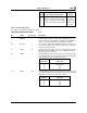
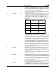
TIR24: TCR Index Register
This register is the TCR Index register. This register is
used as an address into indirect TAI register space. The
value in the TCR Index Register is used as an address
that points at one of 64 registers that are accessed
through the TCR Data Port.
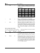
Bit Name Reset Value Description
7:6 Reserved – Reserved. Must be written as a 0. Reads of this bit produce
undefined data.
5:0 TCRI[5:0] 00h TCR Index value. The value in the TCR Index Register is used as an
address that points at one of 64 registers that are accessed through
the TCR Data Port.
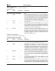
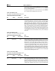
TIR25: Configuration Data Port
This register is the Configuration Data Port register.
This register is used as the data port allowing access
to 64 indirectly accessed registers. The register that is
accessed through the Configuration Data Port is deter-
mined by the current setting of the Configuration Index
Register.
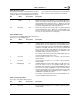
Bit Name Reset Value Description
7–0 CD[7:0] – Configuration Register Data. This register is used as the data port
allowing access to 64 indirectly accessed registers. The register
that is accessed through the Configuration Data Port is determined
by the current setting of the Configuration Index Register.
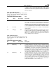
TIR26: Antenna Diversity and A/D Control
This register is the Antenna Diversity and A/D
Control register.
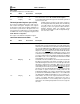
Bit Name Reset Value Description
7 CHBSY 0 Channel Busy. The Am79C930 device will set this bit to a 1 when
the clear channel assessment logic determines that a carrier is pre-
sent. The Am79C930 device will set this bit to a 0 when the clear
channel assessment logic determines that a carrier is not present.
Writes by firmware will have no effect on this bit.
6 ANTLOK 0 Antenna Selection Locked. The Am79C930 device will set
ANTLOK to a 1 when it has determined that criteria for antenna se-
lection have been passed. The Am79C930 device will set ANTLOK
to a 0 when the RXS bit of TIR16 is set 1.
5 ANTSLT 0 Antenna Selection. This bit gives the current value of the ANTSLT
pin, whether determined by register bit programming or internal an-
tenna selection logic. This bit is read only.
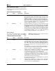
4 ANTS 0 Antenna Switch. If ANTSEN is set to 1, then the software may di-
rectly control the value of the ANTSLT and ANTSLT pins with this
bit. If ANTSEN is set to 0, then writes to this bit will have no effect on
the value of the ANTSLT and ANTSLT pins.
Note: Antenna diversity
is disabled with the ANTSEN bit (bit 3 of TIR26).
3 ANTSEN 0 Antenna Switch Enable. ANTSEN and ANTSLTLFN (TCR30[7])
are combined with the PCMCIA pin setting to determine the func-
tionality of the ANTSLT and ANTSLT pins.
The complete control of the function of the ANTSLT and ANTSLT
pins are described in the
Multi-Function Pin
section.