
- SUPER X6DVA-4G/X6DVA-EG USER'S MANUAL


1-4
Introduction
X6DVA-4G/X6DVA-EG User's Manual
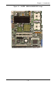
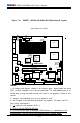
Figure 1-2. SUPER X6DVA-4G/X6DVA-EG Motherboard Layout
GLAN1
®
S
UPER X6DVA-4G
(not drawn to scale)
GLAN2
DIMM 2B
DIMM 2A
DIMM 3B
DIMM 3A
DIMM 1A
DIMM 1B
8-pin
PWR2
SMB
PWR
FP CTRL
Speaker
WOR
GLAN
CTLR
X4 PCI-Epxess
PCIX #6 (PCIX-133)
North
Bridge
VGA
COM1
USB0/1
KB/
Mouse
PW4
ATX
PWR1
24-Pin
Fan1
PW1
CPU 1
CPU 2
COM2
6300ESB
ICH
GLAN
CTLR
PWR
Fault
J2
J3
J4
J1
PW3
J18
J19
J20
J21
J22
J23
J8B1
JPL1
LAN1Enable
JPL2
LAN2Enable
PCIX #5 (PCIX-100)
JPR1
Alarm
Reset
J9B1
J15
J13
JPA1
(*SCSI Enable)
PCIX slots/
SMB Connect
JF2
PWLED/
SPKR
PCI-E#4
J14
Battery
Fan6
Fan5
JPG1
J17
VGA Enable
32- bit PCI #1
J5
Printer
J10
Floppy
J24
SCSI
J28
JL1
IDE 2
J38
Fan4
SATA0
SATA1
JS0
Cha. Intru
JS1
JBT1
Clr CMOS
J41
IPMI
JWD
WD
IDE 1
J44
JF1
Fan3
E7320
(Lindenhurst
-VS)
MCH
PXH
(PCI-E/
PCIX
Interface)
SI/O
VGA
CTLR
SCSI (LSI
53C20)
64- bit
64- bit
USB2,3
JA1
JSLED
SATA
LED
DS9
Fan2
PW2
JWOL
DS7
DS8
POST
LED
System LED
SCSI
ChannelTerm.
Enable
JPF
PWR Force On
BIOS
DS1
DS4
DS2
DS3
CPU
PW LED
CPU1 VRM
OHLED
CPU2 VRM
OH LED
DS5
PWR LED
WOL
SCSI LED
Notes:
1. All images and layouts shown in this manual were based upon the latest
PCB revision available at the time of publishing. The motherboard you’ve re-
ceived may or may not look exactly the same as the graphics shown in this
manual.
2. Jumpers not indicated are for test purposes only.
3. See Chapter 2 for detailed information on jumpers, I/O ports and JF1
front panel connections.
4. " " indicates the location of Pin 1.
5. SCSI is for the X6DVA-4G only.
6. Use the correct type of onboard CMOS battery as specified by the
manufacturer. Do not install the onboard battery upside down.