
Datasheet


AD9523 Data Sheet
Rev. C | Page 10 of 60
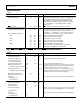
Parameter Min Typ Max Unit Test Conditions/Comments
Current
Input Logic 1 1 µA
Input Logic 0 1 µA
Input Capacitance 2 pF
SDIO, SDO (OUTPUTS)
Output Logic 1 Voltage 2.7 V
Output Logic 0 Voltage 0.4 V
TIMING
Clock Rate (SCLK, 1/t
SCLK
) 25 MHz
Pulse Width High, t
HIGH
8 ns
Pulse Width Low, t
LOW
12
ns
SDIO to SCLK Setup, t
DS
3.3 ns
SCLK to SDIO Hold, t
DH
0 ns
SCLK to Valid SDIO and SDO, t
DV
14 ns
CS
to SCLK Setup, t
S
10 ns
CS
to SCLK Setup and Hold, t
S
, t
C
0 ns
CS
Minimum Pulse Width High, t
PWH
6 ns
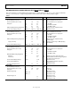
SERIAL CONTROL PORT—I²C MODE
VDD = VDD3_REF, unless otherwise noted.
Table 16.
Parameter Min Typ Max Unit Test Conditions/Comments
SDA, SCL (WHEN INPUTTING DATA)
Input Logic 1 Voltage 0.7 × VDD V
Input Logic 0 Voltage 0.3 × VDD V
Input Current with an Input Voltage Between
0.1 × VDD and 0.9 × VDD
−10 +10 µA
Hysteresis of Schmitt Trigger Inputs
0.015 × VDD
V
Pulse Width of Spikes That Must Be
Suppressed by the Input Filter, t
SPIKE
50 ns
SDA (WHEN OUTPUTTING DATA)
Output Logic 0 Voltage at 3 mA Sink Current 0.4 V
Output Fall Time from VIH
MIN
to VIL
MAX
with
a Bus Capacitance from 10 pF to 400 pF
20 + 0.1 C
B
1
250 ns
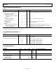
TIMING Note that all I
2
C timing values are referred to
VIH
MIN
(0.3 × VDD) and VIL
MAX
levels (0.7 × VDD)
Clock Rate (SCL, f
I2C
) 400 kHz
Bus Free Time Between a Stop and Start
Condition, t
IDLE
1.3 µs
Setup Time for a Repeated Start Condition, t
SET;
STR
0.6 µs
Hold Time (Repeated) Start Condition, t
HLD; STR
0.6 µs After this period, the first clock pulse is
generated
Setup Time for Stop Condition, t
SET; STP
0.6 µs
Low Period of the SCL Clock, t
LOW
1.3 µs
High Period of the SCL Clock, t
HIGH
0.6 µs
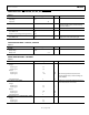
SCL, SDA Rise Time, t
RISE
20 + 0.1 C
B
1
300 ns