
Datasheet


Data Sheet AD9523
Rev. C | Page 7 of 60
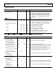
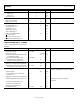
DISTRIBUTION OUTPUT CHARACTERISTICS (OUT0, OUT0 TO OUT13, OUT13)
Duty cycle performance is specified with the invert divider bit set to 1, and the divider phase bits set to 0.5. (For example, for Channel 0,
0x190[7] = 1 and 0x192[7:2] = 1.) Output Voltage Reference VDD in Table 9 refers to the 3.3 VDD3_OUT[x:y] supply.
Table 9.
Parameter Min Typ Max Unit Test Conditions/Comments
LVPECL MODE
Maximum Output Frequency 1 GHz Minimum VCO/maximum dividers
Rise Time/Fall Time (20% to 80%) 117 147 ps 100 Ω termination across output pair
Duty Cycle 47 50 52 % f < 500 MHz
43 48 52 % f = 500 MHz to 800 MHz
40 49 54 % f = 800 MHz to 1 GHz
Differential Output Voltage Magnitude 643 775 924 mV Voltage across pins, output driver static
Common-Mode Output Voltage VDD − 1.5 VDD − 1.4 VDD − 1.25 V Output driver static
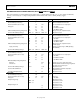
SCALED HSTL MODE, 16 mA
Maximum Output Frequency 1 GHz Minimum VCO/maximum dividers
Rise Time/Fall Time (20% to 80%) 112 141 ps 100 Ω termination across output pair
Duty Cycle 47 50 52 % f < 500 MHz
44 48 51 % f = 500 MHz to 800 MHz
40 49 54 % f = 800 MHz to 1 GHz
Differential Output Voltage Magnitude 1.3 1.6 1.7 V
Voltage across pins, output driver static;
nominal supply
Supply Sensitivity 0.6
mV/
mV
Change in output swing vs. VDD3_OUT[x:y]
(ΔV
OD
/ΔVDD3)
Common-Mode Output Voltage VDD − 1.76 VDD − 1.6 VDD − 1.42 V
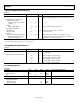
LVDS MODE, 3.5 mA
Maximum Output Frequency 1 GHz
Rise Time/Fall Time (20% to 80%) 138 161 ps 100 Ω termination across output pair
Duty Cycle 48 51 53 % f < 500 MHz
43 49 53 % f = 500 MHz to 800 MHz
41 49 55 % f = 800 MHz to 1 GHz
Differential Output Voltage Magnitude
Balanced 247 454 mV Voltage across pins; output driver static
Unbalanced 50 mV
Absolute difference between voltage magnitude
of normal pin and inverted pin
Common-Mode Output Voltage 1.125 1.375 V Output driver static
Common-Mode Difference 50 mV
Voltage difference between output pins;
output driver static
Short-Circuit Output Current 3.5 24 mA Output driver static
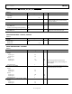
CMOS MODE
Maximum Output Frequency 250 MHz
Rise Time/Fall Time (20% to 80%) 387 665 ps 15 pF load
Duty Cycle 45 50 55 % f = 250 MHz
Output Voltage High Output driver static
VDD − 0.25 V Load current = 10 mA
VDD − 0.1 V Load current = 1 mA
Output Voltage Low Output driver static
0.2 V Load current = 10 mA
0.1 V Load current = 1 mA