
Datasheet


AD9577 Data Sheet
Rev. 0 | Page 2 of 44
TABLE OF CONTENTS
Features .............................................................................................. 1
Applications....................................................................................... 1
General Description......................................................................... 1
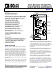
Functional Block Diagram .............................................................. 1
Revision History ............................................................................... 2
Specifications..................................................................................... 3
PLL1 Characteristics .................................................................... 3
PLL1 Clock Output Jitter............................................................. 5
PLL2 Fractional-N Mode Characteristics ................................. 6
PLL2 Integer-N Mode Characteristics....................................... 7
PLL2 Clock Output Jitter............................................................. 9
CMOS Reference Clock Output Jitter...................................... 11
Timing Characteristics .............................................................. 12
Clock Outputs ............................................................................. 13
Power............................................................................................ 14
Crystal Oscillator........................................................................ 15
Reference Input........................................................................... 15
Control Pins ................................................................................ 15
Absolute Maximum Ratings.......................................................... 16
Thermal Characteristics ............................................................ 16
ESD Caution................................................................................ 16
Pin Configuration and Function Descriptions........................... 17
Typical Performance Characteristics ........................................... 19
REFOUT and PLL1 Phase Noise Performance ...................... 19
PLL2 Phase Noise Performance................................................ 20
Output Jitter ................................................................................ 21
Typical Output Signal ................................................................ 22
Typical Spread Spectrum Performance Characteristics........ 24
Terminology .................................................................................... 25
Detailed Block Diagram ................................................................ 27
Example Application.................................................................. 28
Functional Description.................................................................. 29
Reference Input and Reference Dividers................................. 29
Output Channel Dividers.......................................................... 30
Outputs ........................................................................................ 30
Reference Output Buffer ........................................................... 31
PLL1 Integer-N PLL................................................................... 31
PLL1 Phase Frequency Detector (PFD) and Charge Pump . 32
PLL1 VCO ................................................................................... 32
PLL1 Feedback Divider ............................................................. 32
Setting the Output Frequency of PLL1.................................... 32
PLL2 Integer/Fractional-N PLL ............................................... 32
PLL2 Phase Frequency Detector (PFD) and Charge Pump . 33
PLL2 Loop Bandwidth............................................................... 33
PLL2 VCO ................................................................................... 33
PLL2 Feedback Divider ............................................................. 33
PLL2 Σ-Δ Modulator ................................................................. 33
Spur Mechanisms ....................................................................... 33
Optimizing PLL Performance .................................................. 34
Setting the Output Frequency of PLL2.................................... 34
Margining .................................................................................... 35
Spread Spectrum Clock Generation (SSCG).......................... 35
I
2
C Interface Timing and Internal Register Description........... 38
Default Frequency Map and Output Formats ........................ 40
I
2
C Interface Operation ............................................................. 40
Typical Application Circuits ..................................................... 42
Power and Grounding Considerations and Power Supply
Rejection...................................................................................... 43
Outline Dimensions ....................................................................... 44
Ordering Guide .......................................................................... 44
REVISION HISTORY
10/11—Revision 0: Initial Version