
Datasheet


Data Sheet AD9577
Rev. 0 | Page 31 of 44
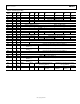
Table 21.PLL2 Output Driver Format Control Bits,
Register DR1[5:3]
FORMAT2 (PLL2)
Register DR1[5:3] OUT3P/OUT3N OUT2P/OUT2N
000 LVPECL LVPECL
001 LVDS LVDS
010 2 × CMOS LVPECL
011 2 × CMOS 2 × CMOS
100 2 × CMOS LVDS
101 LVPECL LVDS
110 LVPECL 2 × CMOS
111
1
2 × CMOS 2 × CMOS
1
This indicates that the CMOS outputs are in phase; otherwise, they are in
antiphase.
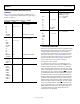
LVDS uses a current mode output stage. The normal value
(default) for this current is 3.5 mA, which yields a 350 mV
output swing across a 100 Ω resistor. The LVDS outputs meet or
exceed all ANSI/TIA/EIA-644 specifications. The LVDS output
buffer should be terminated with a 100 Ω differential resistor
between the receiver input ports (see Figure 38). A recommended
termination circuit for the LVDS outputs is shown in Figure 38.
50Ω
50Ω
LVDS
100Ω
LVDS
09284-042
Figure 38. LVDS Output Termination
See the AN-586 Application Note, LVDS O utputs for High Spee d
A/D Converters, for more information about LVDS.
In a dc-coupled application, the LVPECL output buffer should
be terminated via a pair of 50 Ω resistors to a voltage of V
CC
− 2 V.
This can be implemented by using potential dividers of 127 Ω
and 83 Ω between the supplies, as shown in Figure 39.
3.3V
50Ω
50Ω
SINGLE-ENDED
(NOT COUPLED)
3.3V
3.3
V
LVPECL
127Ω127Ω
83Ω83Ω
V
T
= V
DD
– 2V
LVPECL
09284-043
Figure 39. LVPECL DC-Coupled Termination
An alternative LVPECL termination scheme for dc-coupled
applications is shown Figure 40.
50Ω
50Ω
LVPECL
50Ω
50Ω
50Ω
LVPECL
09284-044
Figure 40. LVPECL DC-Coupled Y-Termination
In ac-coupled applications, the LVPECL output stage needs a
pair of 200 Ω pull-down resistors to GND to provide a dc path for
the output stage emitter followers (see Figure 41). The receiver must
provide an additional 50 Ω single-ended input termination.
50Ω
50Ω
LVPECL
50Ω50Ω
200Ω200Ω
LVPECL
V
TERM
0.1µF
0.1µF
09284-045
Figure 41. LVPECL AC-Coupled Termination
REFERENCE OUTPUT BUFFER
A CMOS buffered copy of the reference input circuit signal is
available at the REFOUT pin. This buffer can be optionally
powered down by setting Register DR2[0], PDRefOut to Logic 0.
PLL1 INTEGER-N PLL
The upper PLL in Figure 32, PLL1, is an integer-N PLL with a
loop bandwidth of 140 kHz. The input frequency to the PLL
from the reference circuit is f
PFD
. The VCO frequency, f
VCO1
, is
programmed by setting the value for Na, according to
f
VCO1
= f
PFD
× Na (3)
where Na is programmable in the 80 to 131 range. The VCO
output frequency can tune over the 2.15 GHz to 2.55 GHz range to
integer multiples of the PFD input frequency only.
By setting each of the VCO divider (V0 and V1) and output
divider (D0 and D1) values, the VCO frequency can be divided
down to the required output frequency, independently, for each
of the output ports, OUT0 and OUT1. The f
OUT0
frequency
presented to OUT0 can be set according to
D0V0
Na
ff
PFD
OUT
×
×=
0
(4)
The frequency f
OUT1
presented to OUT1 can be set according to
11
1
D
V
Na
ff
PFD
OUT
×
×=
(5)
The loop filters required for this PLL are integrated on chip.