
Datasheet


Data Sheet AD9577
Rev. 0 | Page 33 of 44
The f
OUT3
frequency presented to OUT3 can be set according to
D3V3
MOD
FRAC
Nb
ff
PFD
OUT3
×
+
×=
)(
(11)
The loop filters required for this PLL are integrated on chip.
By setting the FRAC value to 0, powering down the SDM by setting
Register ABF0[4] to 1, and turning the bleed current off by setting
Register BP0[2] = 0, PLL2 can operate as an integer-N PLL.
Equation 10 and Equation 11 are still used to set the output
frequencies for f
OUT2
and f
OUT3
. Operation in this mode provides
improved performance in terms of phase noise, spurs, and jitter.
PLL2 PHASE FREQUENCY DETECTOR (PFD) AND
CHARGE PUMP
The PLL2 PFD and charge pump is the same as that described
in the PLL1 Phase Frequency Detector (PFD) and Charge Pump
section. When operating in fractional-N mode, a charge pump
bleed current should be enabled to linearize the PLL transfer
function and, therefore, to minimize spurs due to the operation
of the Σ-Δ modulator. Bleed is enabled by setting Register BP0[2].
PLL2 LOOP BANDWIDTH
The normal PLL loop bandwidth is 50 kHz. When the SSCG input
pin is asserted, the loop bandwidth switches from 50 kHz to
125 kHz, which prevents the triangle-wave modulation waveform
from being overly filtered by the PLL. When the MAX_BW input
pin is set high, it forces the PLL bandwidth to be 250 kHz
instead of 125 kHz.
PLL2 VCO
PLL2 incorporates a low phase noise LC-tank VCO. This VCO
has 32 frequency bands spanning from 2.15 GHz to 2.55 GHz.
At power-up, a VCO calibration cycle begins and the correct band
is selected based on the feedback divider setting (Nb). Whenever a
new feedback divider setting is called for, the VCO calibration
process must run by writing 1 followed by 0 to the NewAcq bit,
Register X0[0].
PLL2 FEEDBACK DIVIDER
The Nb feedback divider ratio is used to set the PLL2 VCO
frequency according to Equation 9. Note that the Nb value is set
by adding the decimal value programmed to Register BF3[5:0]
to a decimal value of 80, where the minimum divider Nb value
is 80. The maximum Nb value is 131. For example, to set Nb to 85,
Register BF3[5:0] is set to 5.
PLL2 Σ-Δ MODULATOR
When operating in fractional-N mode only, PLL2 uses a third-
order, multistage noise shaping (MASH) Σ-Δ modulator (SDM)
to adjust the feedback divider ratio. The programmed Nb value
can be adjusted over the −4 to +3 range on every rising clock
edge from the feedback divider output (typically 25 MHz for
networking applications). In this way, the average feedback divide
ratio is adjusted to be a noninteger value, allowing for a VCO
frequency that is a fractional multiple of the PFD frequency to be
synthesized. By setting the FRAC and MOD values of the SDM, the
PLL2 VCO frequency can be set according to Equation 9. The SDM
must be turned on by setting PD_SDM to 0, Register ABF0[4].
12-Bit Programmable Modulus (MOD) and Fractional
(FRAC) Values
Unlike most other fractional-N PLLs, the AD9577 allows users to
program the modulus over a 12-bit range, which means they can
set up the part in many different configurations. It also usually
means that, in most applications, it is possible to design the PLL
to achieve the desired output frequency multiplication with 0 ppm
frequency error. The MOD value is set by setting Register BF1[3:0]
and Register BF2[7:0]. The FRAC value is set by setting
Register BF0[7:0] and Register BF1[7:4].
Bleed Current
When the SDM is operational (Register ABF0[4] set to 0), bleed
current should be enabled (Register BP0[2] set to 1), which
increases the in-band phase noise but reduces the fractional spur
amplitudes. All fractional-N jitter data is reported with bleed = 1.
If bleed = 0 in fractional-N mode, the rms jitter decreases
significantly; however, the fractional spur amplitudes increase.
When PLL2 operates in integer-N mode, the bleed current
should be disabled to improve the PLLs in-band phase noise.
SPUR MECHANISMS
This section describes the three different spur mechanisms that
arise with a fractional-N PLL: fractional spurs, integer boundary
spurs, and reference spurs.
Fractional Spurs
The fractional interpolator in the AD9577 is a third-order SDM
with a modulus that is programmable to any integer value from
50 to 4095. The SDM is clocked at the PFD reference rate (f
PFD
) that
allows PLL output frequencies to be synthesized at a channel step
resolution of f
PFD
/MOD. The quantization noise from the Σ-Δ
modulator appears as fractional spurs. The interval between spurs
is f
PFD
/L, where L is the repeat length of the code sequence in the
digital Σ-Δ modulator. For the third-order modulator used in the
AD9577, the repeat length depends on the value of MOD, as
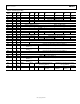
listed in Table 2 3.
Table 23. Fractional Spur Frequencies
Condition
Repeat
Length Spur Interval
If MOD is divisible by 2, but not 3 2 × MOD f
PFD
/(2 × MOD)
If MOD is divisible by 3, but not 2 3 × MOD f
PFD
/(3 × MOD)
If MOD is divisible by 6 6 × MOD f
PFD
/(6 × MOD)
Otherwise MOD f
PFD
/MOD