
Datasheet


Data Sheet AD9577
Rev. 0 | Page 43 of 44
1
10
VSCA
VSI2C
REFOUT
VSREFOUT
VSX
REFCLK
XT2
XT1
REFSEL
VSCB
30
21
OUT3P
VSFB
VSM
SSCG
VSFA
OUT1N
OUT1P
VSOB1A
OUT3N
VSOB3B
11
20
TST1B
TST2B
LDO
G
ND
OUT2N
GND
OUT2P
V
SOB2B
MARGIN
VSVB
OUT0N
O
UT0P
GND
GND
SCL
VSVA
TST2A
40
MAX_BW
VSOB0A
31
SDA
AD9577
22pF
22pF
C
D
C
D
V
S
V
S
V
S
V
S
V
S
V
S
V
S
V
S
C
D
C
D
220nF
C
D
C
D
V
S
V
S
V
S
V
S
V
S
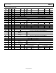
DO NOT CONNECT OTHER TRACES
TO PIN 15, PIN 16, PIN 35, AND PIN 36.
CAPACITORS C
D
CONSIST OF
100nF IN PARALLEL WITH 10nF.
10kΩ
V
S
10kΩ
V
S
50Ω
50Ω
50Ω
50Ω
50Ω
50Ω
V
S
127Ω 83Ω
127Ω 83Ω
V
S
127Ω 83Ω
127Ω 83Ω
V
S
127Ω
83Ω
127Ω
83Ω
50Ω
50Ω
V
S
127Ω
83Ω
127Ω
83Ω
09284-055
C
D
C
D
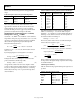
Figure 50. Typical LVPECL Application Circuit
POWER AND GROUNDING CONSIDERATIONS AND POWER SUPPLY REJECTION
Many applications seek high speed and performance under less
than ideal operating conditions. In these application circuits,
the implementation and construction of the PCB is as important
as the circuit design. Proper RF techniques must be used for
device selection, placement, and routing, as well as for power
supply bypassing and grounding to ensure optimum performance.
Each power supply pin should have independent decoupling and
connections to the power supply plane. It is recommended that the
device exposed paddle be directly connected to the ground plane
by a grid of at least nine vias. Care should be taken to ensure that
the output traces cannot couple onto the reference or crystal input
circuitry.