Atmel 8051 Microcontrollers Hardware Manual
Section 1 The C51 Instruction Set ........................................................................ 1-1 1.1 1.2 Program Status Word................................................................................1-1 Addressing Modes ....................................................................................1-2 1.2.1 Direct Addressing ..............................................................................1-2 1.2.2 Indirect Addressing.................................................
Table of Contents 2.5 Port Structures and Operation ................................................................2-23 2.5.1 I/O Configurations............................................................................2-23 2.5.2 Writing to a Port...............................................................................2-24 2.5.3 Port Loading and Interfacing ............................................................2-26 2.5.4 Read-Modify-Write Feature .....................................
Table of Contents 2.15.1 Multiprocessor Communications ......................................................2-54 2.15.2 Given Address ..................................................................................2-54 2.15.3 Broadcast Address ...........................................................................2-55 2.15.4 Reset Addresses ..............................................................................2-55 2.16 Interrupts ..............................................................
Section 1 The 8051 Instruction Set The 8051 instruction set is optimized for 8-bit control applications. It provides a variety of fast addressing modes for accessing the internal RAM to facilitate byte operations on small data structures. The instruction set provides extensive support for one-bit variables as a separate data type, allowing direct bit manipulation in control and logic systems that require Boolean processing.
The 8051 Instruction Set Table 1-1. PSW: Program Status Word Register (MSB) (LSB) CY AC F0 RS1 RS0 OV - Symbol Position CY PSW.7 Carry flag AC PSW.6 Auxiliary Carry flag. (For BCD operations.) F0 PSW.5 Flag 0 (Available to the user for general purposes.) P Name and Significance Register bank Select control bits 1 & 0. Set/cleared by software to determine working register bank (see Note). RS1 PSW.4 RS0 PSW.3 OV PSW.2 Overflow flag. - PSW.1 (reserved) P PSW.0 Parity flag.
The 8051 Instruction Set to point to it. The opcode does this itself. Instructions that refer to the Accumulator as ‘A’ assemble as accumulator-specific opcodes. 1.2.5 Immediate Constants The value of a constant can follow the opcode in Program Memory. For example; MOV A, # 100 loads the Accumulator with the decimal number 100. The same number could be specified in hex digits as 64H. 1.2.6 Indexed Addressing Only Program Memory can be accessed with indexed addressing, and it can only be read.
The 8051 Instruction Set 1.3 Arithmetic Instructions The menu of arithmetic instructions is listed in Table 1-2. The table indicates the addressing modes that can be used with each instruction to access the operand. For example, the ADD A, instruction can be written as: ADD ADD ADD ADD A,7FH (direct addressing) A,@ R0(indirect addressing) A,R7 (register addressing) A,# 127(immediate constant) Table 1-2. A list of the Atmel 8051 Arithmetic Instructions.
The 8051 Instruction Set The DA A instruction is for BCD arithmetic operations. In BCD arithmetic ADD and ADDC instructions should always be followed by a DA A operation, to ensure that the result is also in BCD. Note that DAA will not convert a binary number to BCD. The DA A operation produces a meaningful result only as the second step in the addition of two BCD bytes. 1.4 Logical Instructions Table 1-3 shows the list of logical instructions.
The 8051 Instruction Set Note that Boolean operations can be performed on any byte in the internal Data Memory space without going through the Accumulator. The XRL , # data instruction, for example, offers a quick and easy way to invert port bits, as in XRL P1, #OFFH If the operation is in response to an interrupt, not using the Accumulator saves the time and effort to stack it in the service routine. The Rotate instructions (RL A, RLC A, etc.) shift the Accumulator 1 bit to the left or right.
The 8051 Instruction Set This means the stack can go into the Upper 128, if they are implemented, but not into SFR space. Table 1-4.
The 8051 Instruction Set Table 1-5.
The 8051 Instruction Set repeated for location 2DH. The CJNE instruction (Compare and Jump if Not Equal) is a loop control that will be described later. The loop is executed from LOOP to CJNE for R1 = 2EH, 2DH, 2CH and 2BH. At that point the digit that was originally shifted out on the right has propagated to location 2AH. Since that location should be left with 0s, the lost digit is moved to the Accumulator. 1.
The 8051 Instruction Set MOV A, ENTRY_NUMBER CALLTABLE The subroutine “TABLE” would look like this: TABLE:MOVC A, @A + PC RET The table itself immediately follows the RET (return) instruction in Program Memory. This type of table can have up to 255 entries, numbered 1 through 255. Number 0 cannot be used, because at the time the MOVC instruction is executed, the PC contains the address of the RET instruction. An entry numbered 0 would be the RET opcode itself. Table 1-8. Lookup Table Read Instructions 1.
The 8051 Instruction Set In this example, FLAG is the name of any addressable bit in the lower 128 or SFR space. An I/O line (the LSB of Port 1, in the case) is set or cleared depending on whether the flag bit is 1 or 0. The Carry bit in the PSW is used as the single-bit Accumulator of the Boolean processor. Bit instructions that refer to the Carry bit as C assemble as Carry-specific instructions (CLR C, etc.).
The 8051 Instruction Set The SJMP instruction encodes the destination address as relative offset, as described above. The instruction is 2 bytes long, consisting of the opcode and the relative offset byte. The jump distance is limited to range of -128 to + 127 bytes relative to the instruction following the SJMP. The LJMP instruction encodes the destination address as a 16-bit constant. The instruction is 3 bytes long, consisting of the opcode and two address bytes.
The 8051 Instruction Set done. If there is no interrupt in progress at the time RETI is executed, then the RETI is functionally identical to RET. Table 1-11 shows the list of conditional jumps available to the Atmel 8051 user. All of these jumps specify the destination address by the relative offset method, and so are limited to a jump distance of -128 to + 127 bytes from the instruction following the conditional jump instruction.
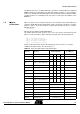
1-14 4316A–8051–01/04 MOV A,R0 1-1 MOVX R0,A 1-1 Fx SUBB A,R0 1-1,C,OV,AC 9x Ex MOV dir,R0 2-2 8x DJNZ R0,rel 2-2 MOV R0,#imm 2-1 7x Dx XRL A,R0 1-1 6x XCH A,R0 1-1 ANL A,R0 1-1 5x Cx ORL A,R0 1-1 4x CJNE R0,#imm,rel 3-2,C ADDC A,R0 1-1,C,OV,AC 3x Bx ADD A,R0 1-1,C,OV,AC 2x MOV R0,dir 2-2 DEC R0 1-1 1x Ax INC R0 1-1 Ox x8 MOVX R1,A 1-1 MOV A,R1 1-1 DJNZ R1,rel 2-2 XCH A,R1 1-1 CJNE R1,#imm,rel 3-2,C MOV R1,dir 2-2 SUBB A,R1 1-1,C,OV,AC MOV dir,R1 2-2 MOV R1,#imm 2-
NOP 1-1 JBC bit,rel 3-2 JB bit,rel 3-2 JNB bit,rel 3-2 JC rel 2-2 JNC rel 2-2 JZ rel 2-2 JNZ rel 2-2 SJMP rel 2-2 MOV DPTR,#imm16 3-2 ORL C,/bit 2-2,C ANL C,/bit 2-2,C PUSH dir 2-2 POP dir 2-2 MOVX A,@DPTR 1-2 MOVX @DPTR,A 1-2 Ox 1x 2x 3x 4x 5x 6x 7x 8x 9x Ax Bx Cx Dx Ex Fx x0 Atmel 8051 Microcontrollers Hardware Manual ACALL addr11 2-2 AJMP addr11 2-2 ACALL addr11 2-2 AJMP addr11 2-2 ACALL addr11 2-2 AJMP addr11 2-2 ACALL addr11 2-2 AJMP addr11 2-2 ACALL addr11 2-2
Atmel 8051 Microcontrollers Hardware Manual 1-16 Rev.
Section 2 Common Features Description 2.1 Introduction This chapter presents a comprehensive description of the on-chip hardware features of the Atmel 8051 microcontrollers. Included in this description are: The port drivers and how they function both as ports and, for Ports 0 and 2, in bus operations The Timer/Counters The serial Interface The Interrupt System Reset The reduced Power Modes Atmel 8051 Microcontrollers Hardware Manual 2-17 Rev.
Common Features Description Figure 2-1. 8051 Architecture Block Diagram Note: (*)For Timer 2 only. Figure 2-1 shows a functional block diagram of the 80C51s. 2.2 Special Function Registers 2-18 4316A–8051–01/04 A map of the on-chip memory area called SFR (Special Function Register) space is shown in Figure 2-1. SFRs marked by parentheses are resident in the microcontroller which have the Timer2 feature.Note that not all of the addresses are occupied.
Common Features Description Table 2-1.
Common Features Description Table 2-2. PSW: Program Status Word Register (MSB) (LSB) CY AC F0 RS1 RS0 OV - Symbol Position CY PSW.7 Carry flag AC PSW.6 Auxiliary Carry flag. (For BCD operations.) F0 PSW.5 Flag 0 (Available to the user for general purposes.) P Name and Significance Register bank Select control bits 1 & 0. Set/cleared by software to determine working register bank (see Note). RS1 PSW.4 RS0 PSW.3 OV PSW.2 Overflow flag. - PSW.1 (reserved) P PSW.
Common Features Description 2.2.10 Control Registers Special Function Registers IP, IE, TMOD, TCON, T2CON, SCON, and PCON contain control and status bits for the interrupt system, the timer/counters, and the serial port. They are described in later sections. 2.3 Oscillator and Clock Circuit XTAL1 and XTAL2 are the input and output of a single-stage on-chip inverter, which can be configured with off-chip components as a Pierce oscillator, as shown in Figure 2-2.
Common Features Description 2.4 CPU Timing 2.4.1 X1 Mode (Standard Mode) A machine cycle consists of 6 states (12 oscillator periods). Each state is divided into a Phase 1 half, during which the Phase 1 clock is active, and a Phase 2 half, during which the Phase 2 clock is active. Thus, a machine cycle consists of 12 oscillator periods, numbered S1P1 (State 1, Phase 1), through S6P2 (State 6, Phase 2). Each phase lasts for one oscillator period. Each state lasts for two oscillator periods.
Common Features Description Figure 2-3. 80C51 fetch/Execute Sequences. 2.4.2 X2 Mode This section not yet available.
Common Features Description 2.5 Port Structures and Operation All four ports in the 80C51 are bidirectional. Each consists of a latch (Special Function Register P0 through P3), an output driver, and an input buffer. The output drivers of Ports 0 and 2, and input buffers of Port 0, are used in accesses to external memory. In this application, Port 0 outputs the low byte of the external memory address, time-multiplexed with the byte being written or read.
Common Features Description Figure 2-4. 80C51 Port Bit Latches and I/O Buffers. As shown in Figure 2-4, the output drivers of Ports 0 and 2 are switchable to an internal ADDR and ADDR/DATA bus by an internal CONTROL signal for use in external memory accesses. During external memory accesses, the P2 SFR remains unchanged, but the P0 SFR gets 1s written to it.
Common Features Description in the data sheets) when externally pulled low. Port 0, on the other hand, is considered “true” bidirectional, because when configured as an input it floats. All the port latches in the 80C51 have 1’s written to them by the reset function. If a 0 is subsequently written to a port latch, it can be re configured as an input by writing a 1 to it. 2.5.
Common Features Description up P2 to drive the transistor. Figure 2-6 shows an example where the port is driven by an open drain transistor tN. The parasitic capacitance is equal to 1000pF. Figure 2-6. Port Interfacing The above diagram show the behavior of the port during 0 to 1 transition. In the area A only pull-up P2 sinks the capacitor and takes 5 µs to switch from 0 volt to 2 volts. In the area B, pull-up P2 and P3 feed the capacitor and the time to charge the capacitor is divide roughly by ten.
Common Features Description CLR PX.Y(clear bit Y of Port X) SETB PX.Y(set bit Y of Port X) It is not obvious that the last three instructions in this list are read-modify-write instructions, but they are. They read the port byte, all 8 bits, modify the addressed bit, then write the new byte back to the latch. The reason that read-modify-write instructions are directed to the latch rather than the pin is to avoid a possible misinterpretation of the voltage level at the pin.
Common Features Description When the CPU is executing out of external Program Memory, all 8 bits of Port 2 are dedicated to an output function and may not be used for general purpose I/O. During external program fetches they output the high byte of the PC. During this time the Port 2 drivers use the strong pull-ups to emit PC bits that are 1’s. Figure 2-8. External Program Memory Execution 2.7 PSEN The read strobe for external fetches is PSEN. PSEN is not activated for internal fetches.
Common Features Description that purpose ALE is activated twice every machine cycle. This activation takes place even when the cycle involves no external fetch. The only time an ALE pulse doesn’t come out is during an access to external Data Memory. The first ALE of the second cycle of a MOVX instructions is missing. The ALE disable mode, described in Section 2.8.2, disables the ALE output.
Common Features Description 2.9 Timer/Counters The Atmel 80C51 Microcontrollers implement two general purpose, 16-bit timers/counters. They are identified as Timer 0 and Timer 1, and can be independently configured to operate in a variety of modes as a timer or as an event counter. When operating as a timer, the timer/counter runs for a programmed length of time, then issues an interrupt request. When operating as a counter, the timer/counter counts negative transitions on an external pin.
Common Features Description For normal timer operation (GATE0= 0), setting TR0 allows TL0 to be incremented by the selected input. Setting GATE0 and TR0 allows external pin INT0# to control timer operation. Timer 0 overflow (count rolls over from all 1s to all 0s) sets TF0 flag, generating an interrupt request. It is important to stop timer/counter before changing mode. 2.10.
Common Features Description Figure 2-10. Timer/Counter x (x = 0 or 1) in Mode 1 PERIPH CLOCK ÷6 0 THx (8 bits) 1 TLx (8 bits) Overflow TFx TCON reg Timer x Interrupt Request Tx C/Tx# TMOD reg INTx# TRx TCON reg GATE 2.10.3 Mode 2 (8-bit Timer with Auto-Reload) Mode 2 configures timer 0 as an 8-bit timer (TL0 register) that automatically reloads from the TH0 register (see Table 2-6 on page 37).
Common Features Description Figure 2-12. Timer/Counter 0 in Mode 3: Two 8-bit Counters PERIPH CLOCK ÷6 0 1 TL0 (8 bits) Overflow TH0 (8 bits) Overflow TF0 TCON.5 Timer 0 Interrupt Request TF1 TCON.7 Timer 1 Interrupt Request T0 C/T0# TMOD.2 INT0# TR0 TCON.4 GATE PERIPH CLOCK ÷6 TR1 TCON.6 2.11 2.11.1 Timer 1 Mode 0 (13-bit Timer) 2-34 4316A–8051–01/04 Timer 1 is identical to timer 0, except for mode 3, which is a hold-count mode.
Common Features Description Figure 2-13. Timer/Counter 1 Mode 0: 13-bit Counter Periph Clock /6 2.11.2 Mode 1 (16-bit Timer) Mode 1 configures Timer 1 as a 16-bit timer with the TH1 and TL1 registers connected in cascade (see Figure 2-10). The selected input increments the TL1 register. 2.11.3 Mode 2 (8-bit Timer with Auto Reload) Mode 2 configures Timer 1 as an 8-bit timer (TL1 register) with automatic reload from the TH1 register on overflow (see Figure 2-11).
Common Features Description Figure 2-15. Timer Interrupt System Timer 0 Interrupt Request TF0 TCON.5 ET0 IE0.1 Timer 1 Interrupt Request TF1 TCON.7 ET1 IE0.3 2.11.6 Timer Registers Table 2-4. TCON Register - TCON (S:88h) Timer/Counter Control Register. 7 6 5 4 3 2 1 0 TF1 TR1 TF0 TR0 IE1 IT1 IE0 IT0 Bit Number Bit Mnemonic Description 7 TF1 Timer 1 Overflow Flag Cleared by hardware when processor vectors to interrupt routine.
Common Features Description Table 2-5. TMOD Register - TMOD (S:89h) Timer/Counter Mode Control Register 7 6 5 4 3 2 1 0 GATE1 C/T1# M11 M01 GATE0 C/T0# M10 M00 Bit Number Bit Mnemonic Description 7 GATE1 Timer 1 Gating Control Bit Clear to enable timer 1 whenever the TR1 bit is set. Set to enable timer 1 only while the INT1# pin is high and TR1 bit is set. 6 C/T1# Timer 1 Counter/Timer Select Bit Clear for timer operation: timer 1 counts the divided-down system clock.
Common Features Description Table 2-7. TL0 Register - TL0 (S:8Ah) Timer 0 Low Byte Register 7 Bit Number 6 5 4 3 2 1 0 3 2 1 0 3 2 1 0 Bit Mnemonic Description 7:0 Low Byte of Timer 0. Reset Value = 0000 0000b Table 2-8. TH1 Register - TH1 (S:8Dh) Timer 1 High Byte Register 7 Bit Number 6 5 4 Bit Mnemonic Description 7:0 High Byte of Timer 1. Reset Value = 0000 0000b Table 2-9.
Common Features Description 2.12 Timer 2 Timer 2 is a 16-bit timer/counter which is present in most of the Atmel 8051 microcontrollers.The count is maintained by two 8-bit timer registers, TH2 and TL2, that are cascade connected. Like Timers 0 and 1, it can operate either as a timer or as an event counter. It is controlled by the T2CON register (See Table 2-11) and the T2MOD register (See Table 2-12). Timer 2 operation is similar to Timer 0 and Timer 1.
Common Features Description but with the added feature that a 1-to-0 transition at external input T2EX will also trigger the 16-bit reload and set EXF2. 2.12.1 Auto-reload Mode The auto-reload mode configures timer 2 as a 16-bit timer or event counter with automatic reload. This feature is controlled by the DCEN bit in the T2MOD register (See Table 2-12). Setting the DCEN bit enables timer 2 to count up or down as shown in Figure 2-17. In this mode the T2EX pin controls the counting direction.
Common Features Description depending on the system oscillator frequency and the value in the RCAP2H and RCAP2L registers: F × 2 x2 osc Clock – OutFrequency = ----------------------------------------------------------------------------------------4 × ( 65536 – RCAP2H ⁄ RCAP2L ) Note: X2 bit is located in the CKCON register. In X2 mode, FOSC=FXTAL. In standard mode, FOSC=FXTAL/2. For a 16 MHz system clock, timer 2 has a programmable frequency range of 61 Hz (FOSC/216) to 4 MHz (FOSC/4).
Common Features Description Bit Number 7 Bit Mnemonic Description TF2 Timer 2 overflow Flag TF2 is not set if RCLK=1 or TCLK = 1. Must be cleared by software. Set by hardware on timer 2 overflow. 6 EXF2 Timer 2 External Flag Set when a capture or a reload is caused by a negative transition on T2EX pin if EXEN2=1. Set to cause the CPU to vector to timer 2 interrupt routine when timer 2 interrupt is enabled. Must be cleared by software.
Common Features Description Table 2-12. T2MOD Register - T2MOD (S:C9h) Timer 2 Mode Control Register 7 6 5 4 3 2 1 0 - - - - - - T2OE DCEN Bit Number Bit Mnemonic Description 7 - Reserved The value read from this bit is indeterminate. Do not set this bit. 6 - Reserved The value read from this bit is indeterminate. Do not set this bit. 5 - Reserved The value read from this bit is indeterminate. Do not set this bit. 4 - Reserved The value read from this bit is indeterminate.
Common Features Description Table 2-14. TL2 Register - TL2 (S:CCh) Timer 2 Low Byte Register 7 6 5 4 3 2 1 0 - - - - - - - - Bit Number Bit Mnemonic Description 7:0 Low Byte of Timer 2. Reset Value = 0000 0000b Not bit addressable Table 2-15. RCAP2H Register -RCAP2H (S:CBh) Timer 2 Reload/Capture High Byte Register 7 6 5 4 3 2 1 0 - - - - - - - - Bit Number Bit Mnemonic Description 7:0 High Byte of Timer 2 Reload/Capture.
Common Features Description The serial port can operate in 4 modes: Mode 0: Serial data enters and exits through RXD. TXD outputs the shift clock. 8 bits are transmitted/received: 8 data bits (LSB first). The baud rate is fixed at 1/12 the oscillator frequency. Mode 1: 10 bits are transmitted (through TXD) or received (through RXD): a start bit (0), 8 data bits (LSB first), and a stop bit (1). On receive, the stop bit goes into RB8 in Special Function Register SCON. The baud rate is variable.
Common Features Description Table 2-17. SCON Register SCON - Serial Control Register (98h) 7 6 5 4 3 2 1 0 FE/SM0 SM1 SM2 REN TB8 RB8 TI RI Bit Bit Number Mnemonic Description Framing Error bit (SMOD0=1) FE Clear to reset the error state, not cleared by a valid stop bit. Set by hardware when an invalid stop bit is detected. SMOD0 must be set to enable access to the FE bit 7 SM0 Serial port Mode bit 0 Refer to SM1 for serial port mode selection.
Common Features Description The baud rate in Mode 2 depends on the value of bit SMOD in Special Function Register PCON. If SMOD = 0 (which is its value on reset), the baud rate is 1/64 the oscillator frequency. If SMOD = 1, the baud rate is 1/32 the oscillator frequency. In the 80C51, the baud rates in Modes 1 and 3 are determined by the Timer 1 overflow rate. In case of Timer2, these baud rates can be determined by Timer 1, or by Timer 2, or by both (one for transmit and the other for receive).
Common Features Description Figure 2-20. Internal Baud Rate Periph Clock FPER /6 0 auto reload counter overflow BRG /2 1 0 INT_BRG 1 BRL SPD SMOD1 BRR • The baud rate for UART is token by formula: Baud_Rate = 2SMOD1 x FPER 6(1-SPD) x 32 x [256 - (BRL)] (BRL) = 256 - 2SMOD1 x FPER 6(1-SPD) x 32 x Baud_Rate Table 2-18. Example of computed value when X2=1, SMOD1=1, SPD=1 Example of computed value when X2=1, SMOD1=1, SPD=1 Baud Rates FOSCA = 16.
Common Features Description 2.13.4 Using Timer 1 to Generate Baud Rates When Timer 1 is used as the baud rate generator, the baud rates in Modes 1 and 3 are determined by the Timer 1 overflow rate and the value of SMOD as follows: The Timer 1 interrupt should be disabled in this application. The Timer itself can be configured for either “timer” or “counter” operation, and in any of its 3 running modes.
Common Features Description Figure 2-22. Timer 2 in Baud Rate Generator Mode. Periph Clock 1 The baud rate generator mode is similar to the auto-reload mode, in that a rollover in TH2 causes the Timer 2 registers to be reloaded with the 16-bit value in registers RCAP2H and RCAP2L, which are preset by software. Now, the baud rates in Modes 1 and 3 are determined by Timer 2’s overflow rate as follows: The Timer can be configured for either “timer” or “counter” operation.
Common Features Description Figure 2-23. Timer 2 Generated Commonly Used Baud Rates Fosc (MHz) 6 11.0592 12 16 Baudrate (RCAP2H RACP2L) 110 F9-57 EE-3F 300 FD-8F FB-80 FB-1E F9-7D 600 FE-C8 FD-C0 FD-8F FC-BF 1200 FF-64 FE-E0 FE-C8 FE-5F 2400 FF-B2 FF-70 FF-64 FF-30 4800 FF-D9 FF-B8 FF-B2 FF-98 9600 FF-DC FF-D9 FF-CC 19200 FF-EE FF-E6 38400 FF-F7 FF-F3 56800 FF-FA XX-XX are values of RCAP2H-RCAP2L 2.13.
Common Features Description As data bits come in from the right, 1’s shift out to the left. When the 0 that was initially loaded into the rightmost position arrives at the leftmost position in the shift and load SBUF. At S1P1 of the 10th machine cycle after the write to SCON that cleared RI, RECEIVE is cleared and RI is set. 2.13.7 More About Mode 1 Ten bits are transmitted (through TXD), or received (through RXD): a start bit (0), 8 data bits (LSB first), and a stop bit (1).
Common Features Description Figure 2-24.
Common Features Description 2.14 Framing Error Detection Framing bit error detection is provided for the three asynchronous modes (modes 1, 2 and 3). To enable the framing bit error detection feature, set SMOD0 bit in PCON register (see Figure 2-25). Figure 2-25.
Common Features Description 2.15 Automatic Address Recognition 2.15.1 Multiprocessor Communications Implemented in hardware, automatic address recognition enhances the multiprocessor communication feature by allowing the serial port to examine the address of each incoming command frame. Only when the serial port recognizes its own address, the receiver sets RI bit in SCON register to generate an interrupt. This ensures that the CPU is not interrupted by command frames addressed to other devices.
Common Features Description Slave C:SADDR1111 0011b SADEN1111 1101b Given1111 00X1b The SADEN byte is selected so that each slave may be addressed separately. For slave A, bit 0 (the LSB) is a don’t-care bit; for slaves B and C, bit 0 is a 1. To communicate with slave A only, the master must send an address where bit 0 is clear (e.g. 1111 0000b). For slave A, bit 1 is a 1; for slaves B and C, bit 1 is a don’t care bit.
Common Features Description Table 2-21.
Common Features Description UART Registers Table 2-22. SCON Register SCON - Serial Control Register (98h) 7 6 5 4 3 2 1 0 FE/SM0 SM1 SM2 REN TB8 RB8 TI RI Bit Bit Number Mnemonic Description Framing Error bit (SMOD0=1) FE Clear to reset the error state, not cleared by a valid stop bit. Set by hardware when an invalid stop bit is detected. SMOD0 must be set to enable access to the FE bit 7 SM0 Serial port Mode bit 0 Refer to SM1 for serial port mode selection.
Common Features Description Table 2-23. SADEN Register SADEN - Slave Address Mask Register for UART (B9h) 7 6 5 4 3 2 1 0 3 2 1 0 3 2 1 0 Reset Value = 0000 0000b Table 2-24. SADDR Register SADDR - Slave Address Register for UART (A9h) 7 6 5 4 Reset Value = 0000 0000b Table 2-25. SBUF Register SBUF - Serial Buffer Register for UART (99h) 7 6 5 4 Reset Value = XXXX XXXXb Table 2-26.
Common Features Description Table 2-27. T2CON Register T2CON - Timer 2 Control Register (C8h) 7 6 5 4 3 2 1 0 TF2 EXF2 RCLK TCLK EXEN2 TR2 C/T2# CP/RL2# Bit Bit Number Mnemonic 7 TF2 Description Timer 2 overflow Flag Must be cleared by software. Set by hardware on timer 2 overflow, if RCLK = 0 and TCLK = 0. 6 EXF2 Timer 2 External Flag Set when a capture or a reload is caused by a negative transition on T2EX pin if EXEN2=1.
Common Features Description Table 2-28. PCON Register PCON - Power Control Register (87h) 7 6 5 4 3 2 1 0 SMOD1 SMOD0 - POF GF1 GF0 PD IDL Bit Bit Number Mnemonic 7 SMOD1 6 SMOD0 5 - 4 POF Power-Off Flag Cleared to recognize next reset type. Set by hardware when VCC rises from 0 to its nominal voltage. Can also be set by software. 3 GF1 General purpose Flag Cleared by user for general purpose usage. Set by user for general purpose usage.
Common Features Description Table 2-29. BDRCON Register BDRCON - Baud Rate Control Register (9Bh) 7 6 5 4 3 2 1 0 - - - BRR TBCK RBCK SPD SRC Bit Number Bit Mnemonic 7 - Reserved The value read from this bit is indeterminate. Do not set this bit 6 - Reserved The value read from this bit is indeterminate. Do not set this bit 5 - Reserved The value read from this bit is indeterminate. Do not set this bit.
Common Features Description 2.16.1 How Interrupts Are Handled The interrupt flags are sampled at SsP2 of every machine cycle. The samples are polled during the following machine cycle. If one of the flags was in a set condition at S5P2 of the preceding cycle, the polling cycle will find it and the interrupt system will generate an LCALL to the appropriate service routine, provided this hardwaregenerated LCALL is not clocked by any of the following conditions: 1.
Common Features Description The hardware-generated LCALL pushes the contents of the Program Counter onto the stack (but it does not save the PSW) and reloads the PC with an address that depends on the source of the interrupt being vectored to, as shown below. Source Vector Address IE0 0003H TF0 000BH IE1 0013H TF1 001BH RI + TI 0023H TF2 + EXF2 002BH Execution proceeds from that location until the RETI instruction is encountered.
Common Features Description complete the instruction in progress, plus 4 cycles to complete the next instruction if the instruction is MUL or DIV). Thus, in a single-interrupt system, the response time is always more than 3 cycles and less than 8 cycles.
Atmel Corporation 2325 Orchard Parkway San Jose, CA 95131, USA Tel: 1(408) 441-0311 Fax: 1(408) 487-2600 Regional Headquarters Europe Atmel Sarl Route des Arsenaux 41 Case Postale 80 CH-1705 Fribourg Switzerland Tel: (41) 26-426-5555 Fax: (41) 26-426-5500 Asia Room 1219 Chinachem Golden Plaza 77 Mody Road Tsimshatsui East Kowloon Hong Kong Tel: (852) 2721-9778 Fax: (852) 2722-1369 Japan 9F, Tonetsu Shinkawa Bldg.