
Hardware manual

The 8051 Instruction Set
1-2 Atmel 8051 Microcontrollers Hardware Manual
4316A–8051–01/04
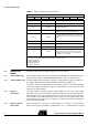
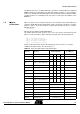
Table 1-1. PSW: Program Status Word Register
1.2 Addressing
Modes
The addressing modes in the 8051 instruction set are as follows:
1.2.1 Direct Addressing In direct addressing the operand is specified by an 8-bit address field in the instruction.
Only 128 Lowest bytes of internal Data RAM and SFRs can be directly addressed.
1.2.2 Indirect Addressing In indirect addressing the instruction specifies a register which contains the address of
the operand. Both internal and external RAM can be indirectly addressed.
The address register for 8-bit addresses can be R0 or R1 of the selected register bank,
or the Stack Pointer. The address register for 16-bit addresses can only be the 16-bit
“data pointer” register, DPTR.
1.2.3 Register
Instructions
The register banks, containing registers R0 through R7, can be accessed by certain
instructions which carry a 3-bit register specification within the opcode of the instruction.
Instructions that access the registers this way are code efficient, since this mode elimi-
nates an address byte. When the instruction is executed, one of the eight registers in the
selected bank is accessed. One of four banks is selected at execution time by the two
bank select bits in the PSW.
1.2.4 Register-specific
Instructions
Some instructions are specific to a certain register. For example, some instructions
always operate on the Accumulator, or Data Pointer, etc., so no address byte is needed
(MSB) (LSB)
CY AC F0 RS1 RS0 OV - P
Symbol Position Name and Significance
CY PSW.7 Carry flag
AC PSW.6
Auxiliary Carry flag.
(For BCD operations.)
F0 PSW.5
Flag 0
(Available to the user for general purposes.)
RS1 PSW.4
Register bank Select control bits 1 & 0. Set/cleared
by software to determine working register bank (see
Note).
RS0 PSW.3
OV PSW.2 Overflow flag.
- PSW.1 (reserved)
PPSW.0
Parity flag.
Set/cleared by hardware each instruction cycle to
indicate and odd/even number of “one” bits in the
accumulator, i.e., even parity.
Note:
The contents of (RS1, RS0) enable the working register banks as follows:
(0.0)-Bank 0(00H-07H)
(0.1)-Bank 1(08H-0FH)
(1.0)-Bank 2(10H-17H)
(1.1)-Bank 3(18H-1FH)