
User Guide


4 Documentation Number ATxWDT-1303
B&B Electronics Mfg Co – 707 Dayton Rd - PO Box 1040 - Ottawa IL 61350 - Ph 815-433-5100 - Fax 815-433-5104
B&B Electronics Ltd – Westlink Comm. Pk – Oranmore, Galway, Ireland – Ph +353 91-792444 – Fax +353 91-792445
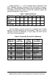
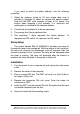
Switch positions 1 - 7 of S1 configure the I/O address of the
WDT. Switches represent a binary 0 in the ON position, a binary 1
when OFF. Least significant bit (LSB) and most significant bit (MSB)
are labeled on the card. Table 1 shows the numerical weight and
electrical connection of each switch.
Table 1. Address Switches
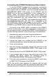
Any I/O address may be used, but it is important that no other
device in the host computer use that address. Table 2 is a list of
frequently unused I/O addresses. In most cases, the WDT can be
set to one of these addresses.
Table 2. Frequently Unused Port Addresses
S1 Position 7 6 5 4 3 2 1
Bus
Connection
SA9 SA8 SA7 SA6 SA5 SA4 SA3
Decimal
Weight
512 256 128 64 32 16 8
Hex Weight 200 100 80 40 20 10 8
Base Hex
Address
Binary
Equivalent
Switch
Settings
MSB LSB
I/O Space
Description
200 1000000000 1000000 game port
208 1000001000 1000001 game port
300 1100000000 1100000 prototype
308 1100001000 1100001 prototype
310 1100010000 1100010 prototype
318 1100011000 1100011 prototype
380 1110000000 1110000 SDLC
388 1110001000 1110001 SDLC
3A0 1110100000 1110100 bisync comm
3A8 1110101000 1110101 bisync comm