
Specifications

LCY-07084A-9
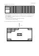
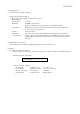
7-3) Timing characteristics of input signals
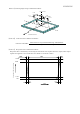
Timing diagrams of input signal are shown in Fig3-1, Fig3-2.
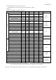
Table7-3
VSHA=5.3V,VSHD=3.3V,GND=0V,Ta=25℃
Parameter Symbol MIN TYP MAX Unit
Terminal
Operating Clock frequency fck − 33.2 34.6 MHz
High level clock width Tcwh 12 − − ns
Low level clock width Tcwl 13 − − ns
Clock rise time Tcr − − 4 ns
Clock fall time Tcf − − 4 ns
CK
[Note7-7]
Start pulse frequency fsp − 31.5 31.8 kHz
Start pulse set up time
Tsusp 4 − − ns
Start pulse hold time
Thsp 0 − − ns
Start pulse width Twsp 1/fck 1/fck 1.5/fck ns
SPR
SPL
[Note7-8]
LS pulse frequency flp − fsp − kHz
LS pulse set up time (CLS) Tsulp 5.0 − − μs
LS pulse set up
time(SPL,SPR)
Tsulpsp
1/fck − − ns
LS pulse hold time(DCLK) Thlpck 20 − − ns
High level LS pulse wide Twlp 1/fck − − ns
LS
Data set up time Tsud 15 − − ns
Source
Data hold time Thd 10 − − ns
R0∼R5,G0∼
G5,B0∼B5
Operating Clock frequency fcls − fsp − kHz
Clock pulse with Twl 5.5 − − μs
Clock rise time Trcl − − 1/fck ns
Clock fall time Tfcl − − 1/fck ns
CLS
Start pulse frequency fsps − 60 65 Hz
Start pulse set up time Tsusps 100 − − ns
Start pulse hold time Thsps 300 − − ns
Start pulse rise time Trsps − − 100 ns
Gate
Start pulse fall time Tfsps − − 100 ns
SPS
COM signal set up time Tsucom
3 − − μs
COM signal hold time Thcom 0 − − μs
COM signal rise time Trcom − − 2 μs
COM signal fall time Tfcom − − 2 μs
VCOM
CS
V0∼V10 signal set up time Tsuv0 3 − − μs
V0∼V10 signal hold time Thv0 0 − − μs
V0∼V10 signal rise time Trv0 − − 2 μs
V0∼V10 signal fall time Tfv0 − − 2 μs
V0,V1,V2,V3,
V4,V5,V6,
V7,V8,V9,V10
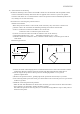
[Note7-7] It is also possible that Tcr,Tcf exceeds the maximum value when the clock frequency
doesn't reach the maximum value. But please confirm there is no problem.
[Note7-8] The rising pulse in CK is existed only 1 time during Hi period (Twsp) on start pulse.