
Specifications
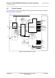
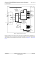
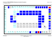
Table Of Contents
- Contents
- Tables
- Figures
- 1 Introduction
- 2 Interface Characteristics
- 2.1 Application Interface
- 2.2 RF Antenna Interface
- 2.3 GNSS Interface
- 2.4 Sample Application
- 3 Operating Characteristics
- 3.1 Operating Modes
- 3.2 Power Up/Power Down Scenarios
- 3.3 Power Saving
- 3.4 Power Supply
- 3.5 Operating Temperatures
- 3.6 Electrostatic Discharge
- 3.7 Blocking against RF on Interface Lines
- 3.8 Reliability Characteristics
- 4 Mechanical Dimensions, Mounting and Packaging
- 5 Regulatory and Type Approval Information
- 6 Document Information
- 7 Appendix

Cinterion
®
EXS62-W/EXS82-W Hardware Interface Description
1.4 Circuit Concept
15
t EXS62-W_EXS82-W_HID_v01.200ee 2022-09-07
Public/ Released
Page 15 of 144
Figure 3: EXS62-W ResM block diagram
Please note that the I
2
C function and some GPIO lines are available with the embedded pro-
cessing option only. Also, some GPIO lines may be shared with further functions that are also
only available with the embedded processing option. For details see Section 2.1, and Section
2.1.8.1.
19.2MHz
32.768kHz
19.2MHz
with
Temp.Sensor
X-tal:
Control interface
Reset
HWID’s
GPIO’s
GNSS
LTE
Antenna LGA Pads
LGA Pads
Baseband controller
with integrated memory
ADC
RF
Interrupt
RF Transceiver
LTE PA+ASM
3
4
Power Management
IC
Power Supply
Power Supply
Serial (ASC0)
Serial (ASC1/GPIO)
USB 2.0
USIM
CCIN
FST_SHDN
STATUS (GPIO)
SUSPEND_MON
SIM_SWITCH(GPIO)
GPIO (not shared)
I
2
C
SPI (GPIO)
VUSIM
ADC1
EMERG_RST
ON
V180
VCORE
BATT+
RF
BATT+
BB
eUICC (option)
8
I/Q-signals
(2x2)
SDR_ASM_ANT
RF_CLK1
SDR_GNSS
BATT+
PS_HOLD
REFE 1...2_
CLK_DATA
4
GPDATA
STMR_SYNC
BATT +
IN
EN
OUT
LDO
USB_VDDA
_3P3
GPIO
RF Part
eUICC
(MFF-XS UICC)
5
Coupler
TX_PA1(LTE_LB)
Matching
GN SS
SAW filter
B71_RX
LB LPF
3
7
2
4
BATT+_RF