COP8SAA5,COP8SAA7,COP8SAB5,COP8SAB7, COP8SAC5,COP8SAC7 COP8SA Family 8-Bit CMOS ROM Based and One-Time Programmable (OTP) Microcontroller with 1k to 4k Memory, Power On Reset, and Very Small Packaging Literature Number: SNOS878E
November 2000 COP8SA Family 8-Bit CMOS ROM Based and One-Time Programmable (OTP) Microcontroller with 1k to 4k Memory, Power On Reset, and Very Small Packaging General Description Note: COP8SAx devices are instruction set and pin compatible supersets of the COP800 Family devices, and are replacements for these in new designs when possible. The COPSAx Rom based and OTP microcontrollers are highly integrated COP8™ feature core devices, with 1k to 4k memory and advanced features including low EMI.
COP8SA Family CPU Features I/O Features n Versatile easy to use instruction set n 1 µs instruction cycle time n Eight multi-source vectored interrupts servicing — External interrupt — Idle Timer T0 — One Timer (with 2 interrupts) — MICROWIRE/PLUS Serial Interface — Multi-Input Wake Up — Software Trap — Default VIS (default interrupt) n 8-bit Stack Pointer SP (stack in RAM) n Two 8-bit Register Indirect Data Memory Pointers n True bit manipulation n Memory mapped I/O n BCD arithmetic instructions n Softw
Single Byte/Single Cycle Code Execution The efficiency is due to the fact that the majority of instructions are of the single byte variety, resulting in minimum program space. Because compact code does not occupy a substantial amount of program memory space, designers can integrate additional features and functionality into the microcontroller program memory space. Also, the majority instructions executed by the device are single cycle, resulting in minimum program execution time.
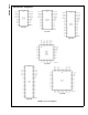
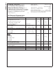
COP8SA Family Connection Diagrams DS012838-2 Top View DS012838-3 Top View DS012838-4 Top View DS012838-39 Top View DS012838-6 Top View DS012838-5 Top View FIGURE 2. Connection Diagrams www.national.
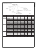
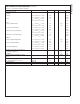
COP8SA Family Ordering Information DS012838-8 FIGURE 3.
COP8SA Family Ordering Information (Continued) Voltage at Any Pin ESD Protection Level 4.0 Electrical Characteristics Total Current into VCC Pin (Source) Total Current out of GND Pin (Sink) Storage Temperature Range Absolute Maximum Ratings (Note 1) If Military/Aerospace specified devices are required, please contact the National Semiconductor Sales Office/ Distributors for availability and specifications. Supply Voltage (VCC) −0.6V to VCC +0.
(Continued) 0˚C ≤ TA ≤ +70˚C unless otherwise specified. Parameter Conditions Min Typ Max Units Output Current Levels D Outputs Source Sink VCC = 4.5V, VOH = 3.3V −0.4 mA VCC = 2.7V, VOH = 1.8V −0.2 mA VCC = 4.5V, VOL = 1.0V 10 mA VCC = 2.7V, VOL = 0.4V 2 mA L Port Source (Weak Pull-Up) Source (Push-Pull Mode) Sink (L0–L3, Push-Pull Mode) Sink (L4–L7, Push-Pull Mode) VCC = 4.5V, VOH = 2.7V −10 −110 µA VCC = 2.7V, VOH = 1.8V −2.5 −33 µA VCC = 4.5V, VOH = 3.3V −0.4 mA VCC = 2.
COP8SA Family AC Electrical Characteristics 0˚C ≤ TA ≤ +70˚C unless otherwise specified. Parameter Conditions Min Typ Max Units DC µs DC µs Instruction Cycle Time (tC) Crystal/Resonator, External Internal R/C Oscillator 4.5V ≤ VCC ≤ 5.5V 1.0 2.7V ≤ VCC 2.0 < 4.5V 4.5V ≤ VCC ≤ 5.5V 1.667 2.7V ≤ VCC < 4.5V TBD R/C Oscillator Frequency Variation 4.5V ≤ VCC ≤ 5.5V (Note 8) 2.7V ≤ VCC < 4.
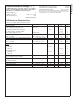
Total Current into VCC Pin (Source) Total Current out of GND Pin (Sink) Storage Temperature Range If Military/Aerospace specified devices are required, please contact the National Semiconductor Sales Office/ Distributors for availability and specifications. Supply Voltage (VCC) Voltage at Any Pin ESD Protection Level 80 mA 100 mA −65˚C to +140˚C Note 10: Absolute maximum ratings indicate limits beyond which damage to the device may occur.
COP8SA Family DC Electrical Characteristics (Continued) −40˚C ≤ TA ≤ +85˚C unless otherwise specified. Parameter Conditions Min Typ Max Units Output Current Levels D Outputs Source Sink VCC = 4.5V, VOH = 3.3V −0.4 mA VCC = 2.7V, VOH = 1.8V −0.2 mA VCC = 4.5V, VOL = 1.0V 10 mA VCC = 2.7V, VOL = 0.4V 2 mA L Port Source (Weak Pull-Up) Source (Push-Pull Mode) Sink (L0–L3, Push-Pull Mode) Sink (L4–L7, Push-Pull Mode) VCC = 4.5V, VOH = 2.7V −10.0 −110 µA VCC = 2.7V, VOH = 1.8V −2.
(Continued) −40˚C ≤ TA ≤ +85˚C unless otherwise specified. Parameter Conditions Min Typ Max Units Inputs tSETUP 4.5V ≤ VCC ≤ 5.5V 200 2.7V ≤ VCC < 4.5V 500 ns tHOLD 4.5V ≤ VCC ≤ 5.5V 60 ns 2.7V ≤ VCC < 4.5V 150 ns Output Propagation Delay (Note 16) ns RL = 2.2k, CL = 100 pF tPD1, tPD0 SO, SK All Others 4.5V ≤ VCC ≤ 5.5V 0.7 µs 2.7V ≤ VCC < 4.5V 1.75 µs 4.5V ≤ VCC ≤ 5.5V 1.0 µs 2.7V ≤ VCC < 4.5V 2.
COP8SA Family Absolute Maximum Ratings (Note 19) Total Current into VCC Pin (Source) Total Current out of GND Pin (Sink) Storage Temperature Range If Military/Aerospace specified devices are required, please contact the National Semiconductor Sales Office/ Distributors for availability and specifications. Supply Voltage (VCC) Voltage at Any Pin ESD Protection Level 80 mA 100 mA −65˚C to +140˚C Note 19: Absolute maximum ratings indicate limits beyond which damage to the device may occur.
(Continued) −40˚C ≤ TA ≤ +125˚C unless otherwise specified. Parameter Conditions Min Typ Max Units 15 mA 3 mA ± 200 mA Allowable Sink Current per Pin (Note 17) D Outputs and L0 to L3 All Others Maximum Input Current without Latchup Room Temp (Note 15) RAM Retention Voltage, Vr 2.0 V 12 µs VCC Rise Time from a VCC ≥ 2.0V (Note 18) Input Capacitance (Note 17) 7 pF Load Capacitance on D2 (Note 17) 1000 pF Typ Max Units DC µs 1.
COP8SA Family The pin is a general purpose I/O if WATCHDOG feature is not selected. If WATCHDOG feature is selected, bit 1 of the Port G configuration and data register does not have any effect on Pin G1 setup. Pin G7 is either input or output depending on the oscillator option selected. With the crystal oscillator option selected, G7 serves as the dedicated output pin for the CKO clock output.
6.0 Functional Description (Continued) The architecture of the device is a modified Harvard architecture. With the Harvard architecture, the program memory EPROM is separated from the data store memory (RAM). Both EPROM and RAM have their own separate addressing space with separate address buses. The architecture, though based on the Harvard architecture, permits transfer of data from EPROM to RAM. 6.
COP8SA Family 6.0 Functional Description 6.5 USER STORAGE SPACE IN EPROM (Continued) In addition to the ECON register, there are 8 bytes of EPROM available for “user information”. ECON and these 8 bytes are outside of the code area and are not protected by the security bit of the ECON register.
frequency at the termination of reset. A Clock Monitor error will cause an active low error output on pin G1. This error output will continue until 16 tC–32 tC clock cycles following the clock frequency reaching the minimum specified value, at which time the G1 output will go high. (Continued) 6.7 RESET The device is initialized when the RESET pin is pulled low or the On-chip Power-On Reset is enabled. 6.7.1 External Reset The RESET input when pulled low initializes the device.
COP8SA Family 6.0 Functional Description 6.8.1 Crystal Oscillator (Continued) The crystal Oscillator mode can be selected by programming ECON Bit 4 to 1. CKI is the clock input while G7/CKO is the clock generator output to the crystal. An on-chip bias resistor connected between CKI and CKO can be enabled by programming ECON Bit 3 to 1 with the crystal oscillator option selection. The value of the resistor is in the range of 0.5M to 2M (typically 1.0M).
COP8SA Family 6.0 Functional Description (Continued) With On-Chip Bias Resistor Without On-Chip Bias Resistor DS012838-17 DS012838-18 FIGURE 12. Crystal Oscillator DS012838-19 FIGURE 13. External Oscillator DS012838-20 DS012838-21 For operation at lower than maximum R/C oscillator frequency. For operation at maximum R/C oscillator frequency. FIGURE 14. R/C Oscillator 19 www.national.
COP8SA Family 6.0 Functional Description T1ENB (Continued) Timer T1 Interrupt Enable for T1B Input capture edge 6.9 CONTROL REGISTERS 7.0 Timers CNTRL Register (Address X'00EE) T1C3 T1C2 T1C1 T1C0 MSEL IEDG SL1 Bit 7 The device contains a very versatile set of timers (T0, T1). Timer T1 and associated autoreload/capture registers power up containing random data.
Underflows from the timer are alternately latched into two pending flags, T1PNDA and T1PNDB. The user must reset these pending flags under software control. Two control enable flags, T1ENA and T1ENB, allow the interrupts from the timer underflow to be enabled or disabled. Setting the timer enable flag T1ENA will cause an interrupt when a timer underflow causes the R1A register to be reloaded into the timer.
COP8SA Family 7.0 Timers fied either as a positive or a negative edge. The trigger condition for each input pin can be specified independently. (Continued) 7.2.3 Mode 3. Input Capture Mode The trigger conditions can also be programmed to generate interrupts. The occurrence of the specified trigger condition on the T1A and T1B pins will be respectively latched into the pending flags, T1PNDA and T1PNDB. The control flag T1ENA allows the interrupt on T1A to be either enabled or disabled.
COP8SA Family 7.0 Timers T1PNDA Timer Interrupt Pending Flag (Continued) T1ENA 7.3 TIMER CONTROL FLAGS The control bits and their functions are summarized below.
COP8SA Family with a low to high transition on the CKO (G7) pin. This method precludes the use of the crystal clock configuration (since CKO becomes a dedicated output), and so may only be used with an R/C clock configuration. The third method of exiting the HALT mode is by pulling the RESET pin low.
COP8SA Family 8.0 Power Save Modes (Continued) DS012838-25 FIGURE 18. Wakeup from HALT 8.2 IDLE MODE The device is placed in the IDLE mode by writing a “1” to the IDLE flag (G6 data bit). In this mode, all activities, except the associated on-board oscillator circuitry and the IDLE Timer T0, are stopped. As with the HALT mode, the device can be returned to normal operation with a reset, or with a Multi-Input Wakeup from the L Port.
COP8SA Family 8.0 Power Save Modes An example may serve to clarify this procedure. Suppose we wish to change the edge select from positive (low going high) to negative (high going low) for L Port bit 5, where bit 5 has previously been enabled for an input interrupt. The program would be as follows: (Continued) 8.3 MULTI-INPUT WAKEUP The Multi-Input Wakeup feature is used to return (wakeup) the device from either the HALT or IDLE modes.
The Software trap has the highest priority while the default VIS has the lowest priority. 9.1 INTRODUCTION Each of the six maskable inputs has a fixed arbitration ranking and vector. The device supports eight vectored interrupts. Interrupt sources include Timer 1, Timer T0, Port L Wakeup, Software Trap, MICROWIRE/PLUS, and External Input. Figure 21 shows the Interrupt Block Diagram. All interrupts force a branch to location 00FF Hex in program memory.
COP8SA Family 9.0 Interrupts interrupt, and jump to the interrupt handling routine corresponding to the highest priority enabled and active interrupt. Alternately, the user may choose to poll all interrupt pending and enable bits to determine the source(s) of the interrupt. If more than one interrupt is active, the user’s program must decide which interrupt to service. (Continued) 9.2 MASKABLE INTERRUPTS All interrupts other than the Software Trap are maskable.
gram context (A, B, X, etc.) and executing the RETI instruction, an interrupt service routine can be terminated by returning to the VIS instruction. In this case, interrupts will be serviced in turn until no further interrupts are pending and the default VIS routine is started. After testing the GIE bit to ensure that execution is not erroneous, the routine should restore the program context and execute the RETI to return to the interrupted program.
COP8SA Family 9.0 Interrupts remains unchanged. The new PC is therefore pointing to the vector of the active interrupt with the highest arbitration ranking. This vector is read from program memory and placed into the PC which is now pointed to the 1st instruction of the service routine of the active interrupt with the highest arbitration ranking. (Continued) 9.3.1 VIS Execution When the VIS instruction is executed it activates the arbitration logic.
COP8SA Family 9.0 Interrupts (Continued) DS012838-30 FIGURE 23. VIS Flowchart 31 www.national.
COP8SA Family 9.0 Interrupts (Continued) Programming Example: External Interrupt WAIT: PSW CNTRL RBIT RBIT SBIT SBIT SBIT JP . . . .=0FF VIS =00EF =00EE 0,PORTGC 0,PORTGD IEDG, CNTRL GIE, PSW EXEN, PSW WAIT . . . .=01FA .
Programming a return to normal execution requires careful consideration. If the Software Trap routine is interrupted by another Software Trap, the RPND instruction in the service routine for the second Software Trap will reset the STPND flag; upon return to the first Software Trap routine, the STPND flag will have the wrong state. This will allow maskable interrupts to be acknowledged during the servicing of the first Software Trap.
COP8SA Family 10.2 WATCHDOG/CLOCK MONITOR OPERATION 10.0 WATCHDOG/Clock Monitor The WATCHDOG is enabled by bit 2 of the ECON register. When this ECON bit is 0, the WATCHDOG is enabled and pin G1 becomes the WATCHDOG output with a weak pullup. The devices contain a user selectable WATCHDOG and clock monitor. The following section is applicable only if WATCHDOG feature has been selected in the ECON register.
COP8SA Family 10.0 WATCHDOG/Clock Monitor (Continued) TABLE 8. WATCHDOG Service Actions Key Window Clock Data Data Monitor Match Match Match Action Valid Service: Restart Service Window Don’t Care Mismatch Don’t Care Error: Generate WATCHDOG Output Mismatch Don’t Care Don’t Care Error: Generate WATCHDOG Output Don’t Care Don’t Care Mismatch Error: Generate WATCHDOG Output 10.
COP8SA Family 11.1 MICROWIRE/PLUS OPERATION 11.0 MICROWIRE/PLUS Setting the BUSY bit in the PSW register causes the MICROWIRE/PLUS to start shifting the data. It gets reset when eight data bits have been shifted. The user may reset the BUSY bit by software to allow less than 8 bits to shift. If enabled, an interrupt is generated when eight data bits have been shifted. The device may enter the MICROWIRE/PLUS mode either as a Master or as a Slave.
The user must set the BUSY flag immediately upon entering the Slave mode. This ensures that all data bits sent by the Master is shifted properly. After eight clock pulses the BUSY flag is clear, the shift clock is stopped, and the sequence may be repeated. (Continued) 11.1.2 MICROWIRE/PLUS Slave Mode Operation In the MICROWIRE/PLUS Slave mode of operation the SK clock is generated by an external source. Setting the MSEL bit in the CNTRL register enables the SO and SK functions onto the G Port.
COP8SA Family 11.0 MICROWIRE/PLUS (Continued) DS012838-35 FIGURE 27. MICROWIRE/PLUS SPI Mode Interface Timing, Normal SK Mode, SK Idle Phase being High DS012838-31 FIGURE 28. MICROWIRE/PLUS SPI Mode Interface Timing, Alternate SK Mode, SK Idle Phase being High www.national.
COP8SA Family 12.0 Memory Map All RAM, ports and registers (except A and PC) are mapped into data memory address space. RAM Address Select ADD REG Contents 64 On-Chip RAM Bytes.
COP8SA Family • • 13.0 Instruction Set 13.1 INTRODUCTION Register B or X Indirect Register B or X Indirect with Post-Incrementing/ Decrementing • Immediate • Immediate Short • Indirect from Program Memory The addressing modes are described below. Each description includes an example of an assembly language instruction using the described addressing mode. Direct. The memory address is specified directly as a byte in the instruction.
The available transfer-of-control addressing modes are: (Continued) • Jump Relative • Jump Absolute • Jump Absolute Long • Jump Indirect The transfer-of-control addressing modes are described below. Each description includes an example of a Jump instruction using a particular addressing mode, and the effect on the Program Counter bytes of executing that instruction. Jump Relative.
COP8SA Family 13.0 Instruction Set Jump to Subroutine Long (JSRL) (Continued) Return from Subroutine (RET) Jump Indirect. In this 1-byte instruction, the lower byte of the jump address is obtained from a table stored in program memory, with the Accumulator serving as the low order byte of a pointer into program memory. For purposes of accessing program memory, the contents of the Accumulator are written to PCL (temporarily).
COP8SA Family 13.0 Instruction Set (Continued) 13.4.9 No-Operation Instruction The no-operation instruction does nothing, except to occupy space in the program memory and time in execution. No-Operation (NOP) Note: The VIS is a special case of the Indirect Transfer of Control addressing mode, where the double byte vector associated with the interrupt is transferred from adjacent addresses in the program memory into the program counter (PC) in order to jump to the associated interrupt service routine.
COP8SA Family 13.0 Instruction Set (Continued) 13.6 INSTRUCTION SET SUMMARY ADD A,Meml ADD ADC A,Meml ADD with Carry SUBC A,Meml Subtract with Carry A← A + Meml A← A + Meml + C, C← Carry, HC← Half Carry A← A − MemI + C, C← Carry, HC← Half Carry AND A,Meml Logical AND A← A and Meml ANDSZ A,Imm Logical AND Immed.
(Continued) JSRL Addr. Jump SubRoutine Long JSR Addr. Jump SubRoutine [SP]← PL, [SP−1]← PU,SP−2, PC← ii [SP]← PL, [SP−1]← PU,SP−2, PC9…0← i PL← ROM (PU,A) JID Jump InDirect RET RETurn from subroutine RETSK RETurn and SKip SP + 2, PL← [SP], PU← [SP−1] SP + 2, PL← [SP],PU← [SP−1], RETI RETurn from Interrupt skip next instruction SP + 2, PL ← [SP],PU← [SP−1],GIE← 1 INTR Generate an Interrupt NOP No OPeration [SP]← PL, [SP−1]← PU, SP−2, PC← 0FF PC← PC + 1 13.
COP8SA Family 13.0 Instruction Set (Continued) Memory Transfer Instructions Register Direct Immed. Indirect [B] [X] X A, (Note 21) 1/1 1/3 2/3 LD A, (Note 21) 1/1 1/3 2/3 2/2 [B+, B−] [X+, X−] 1/2 1/3 1/2 1/3 LD B, Imm 1/1 (If B < 16) LD B, Imm 2/2 (If B > 15) LD Mem, Imm Note 21: = Register Indirect Auto Incr. & Decr. 2/2 3/3 LD Reg, Imm 2/3 IFEQ MD, Imm 3/3 2/2 > Memory location addressed by B or X or directly. www.national.
JP−18 JP−17 JP−16 JP−2 JP−1 JP−0 LD 0FF, #i LD 0FE, #i LD 0FD, #i LD 0FC, #i LD 0FB, #i LD 0FA, #i LD 0F9, #i LD 0F8, #i LD 0F7, #i LD 0F6, #i LD 0F5, #i LD 0F4, #i LD 0F3, #i LD 0F2, #i LD 0F1, #i LD 0F0, #i D DRSZ 0FF DRSZ 0FE DRSZ 0FD DRSZ 0FC DRSZ 0FB DRSZ 0FA DRSZ 0F9 DRSZ 0F8 DRSZ 0F7 DRSZ 0F6 DRSZ 0F5 DRSZ 0F4 DRSZ 0F3 DRSZ 0F2 DRSZ 0F1 DRSZ 0F0 C B * LD A,[X] DIR LD Md,#i LD A,[X−] LD A,[X+] IFNE A,[B] NOP * X A,[X] RPND VIS X A,[X−] X A,[X+] *
COP8SA Family 14.0 Mask Options For mask options information on COP8SAx5 devices, please refer to Section 6.4 ECON (CONFIGURATION) REGISTER. • 15.0 Development Tools Support 15.1 OVERVIEW National is engaged with an international community of independent 3rd party vendors who provide hardware and software development tool support. Through National’s interaction and guidance, these tools cooperate to form a choice of solutions that fits each developer’s needs.
• (Continued) • COP8-UTILS: Free set of COP8 assembly code examples, device drivers, and utilities to speed up code development. COP8 Device Programmer Support • COP8-MLSIM: Free Instruction Level Simulator tool for Windows. For testing and debugging software instructions only (No I/O or interrupt support). COP8 Real-Time Emulation Tools • IM-COP8: MetaLink iceMASTER ® . A full featured, realtime in-circuit emulator for COP8 devices.
COP8SA Family 15.0 Development Tools Support MetaLink COP8-DM (Continued) DM5-KCOP8-SA M Included p/s (PS-10), target cables (DIP and PLCC), 16/20/28/40 DIP/SO and 44 PLCC programming sockets. Add OTP adapter (if needed) and target adapter (if needed) DM Target Adapters MHW-CNVxx (xx = 33, 34 etc.) L DM target converters for 16DIP/20SO/28SO/44QFP/28CSP; (i.e.
(Continued) 15.4 WHERE TO GET TOOLS Tools are ordered directly from the following vendors. Please go to the vendor’s web site for current listings of distributors. Vendor Aisys Home Office Electronic Sites U.S.A.: Santa Clara, CA www.aisysinc.com 1-408-327-8820 info@aisysinc.com Other Main Offices Distributors fax: 1-408-327-8830 Byte Craft U.S.A. www.bytecraft.com 1-519-888-6911 info@bytecraft.com Distributors fax: 1-519-746-6751 IAR Sweden: Uppsala www.iar.se U.S.A.
COP8SA Family Physical Dimensions inches (millimeters) unless otherwise noted 20-Lead Hermetic Dual-In-Line Package, EPROM (D) Order Number COP8SAC720Q3 NS Package Number D20CQ www.national.
COP8SA Family Physical Dimensions inches (millimeters) unless otherwise noted (Continued) Molded Small Outline Package (WM) Order Number COP8SAA716M8 or COP8SAA716M9 NS Package Number M16B Molded Dual-In-Line Package (N) Order Number COP8SAA716N8 or COP8SAA716N9 NS Package Number N16A 53 www.national.
COP8SA Family Physical Dimensions inches (millimeters) unless otherwise noted (Continued) Molded SO Wide Body Package (WM) Order Number COP8SAA720M9, COP8SAB720M9, COP8SAC720M9 COP8SAA720M8, COP8SAB720M8 or COP8SAC720M8 NS Package Number M20B Molded Dual-In-Line Package (N) Order Number COP8SAA720N9, COP8SAB720N9, COP8SAC720N9, COP8SAA720N8, COP8SAB720N8 or COP8SAC720N8 NS Package Number N20A www.national.
COP8SA Family Physical Dimensions inches (millimeters) unless otherwise noted (Continued) 28-Lead Hermetic Dual-In-Line Package EPROM (D) Order Number COP8SAC728Q3 NS Package Number D28JQ 55 www.national.
COP8SA Family Physical Dimensions inches (millimeters) unless otherwise noted (Continued) Molded SO Wide Body Package (WM) Order Number COP8SAA728M9, COP8SAB728M9, COP8SAC728M9, COP8SAA728M8, COP8SAB728M8 or COP8SAC728M8 NS Package Number M28B Molded Dual-In-Line Package (N), Order Number COP8SAA728N9, COP8SAB728N9, COP8SAC728N9, COP8SAA728N8, COP8SAB728N8 or COP8SAC728N8 NS Package Number N28B www.national.
COP8SA Family Physical Dimensions inches (millimeters) unless otherwise noted (Continued) 28 Lead Chip Scale Package (SLB) Order Number COP8SAA7SLB9, COP8SAB7SLB9 or COP8SAC7SLB9 NS Package Number SLB28A 57 www.national.
COP8SA Family Physical Dimensions inches (millimeters) unless otherwise noted (Continued) 40-Lead Hermetic DIP EPROM (D) Order Number COP8SAC740Q3 NS Package Number D40KQ Molded Dual-In-Line Package (N) Order Number COP8SAC740N9 or COP8SAC740N8 NS Package Number N40A www.national.
COP8SA Family Physical Dimensions inches (millimeters) unless otherwise noted (Continued) 44-Lead EPROM Leaded Chip Carrier (EL) Order Number COP8SAC744Q3 NS Package Number EL44C 59 www.national.
COP8SA Family, 8-Bit CMOS ROM Based and One-Time Programmable (OTP) Microcontroller with 1k to 4k Memory, Power On Reset, and Very Small Packaging Physical Dimensions inches (millimeters) unless otherwise noted (Continued) Molded Dual-In-Line Package (N) Order Number COP8SAC744V9 or COP8SAC744V8 NS Package Number V44A LIFE SUPPORT POLICY NATIONAL’S PRODUCTS ARE NOT AUTHORIZED FOR USE AS CRITICAL COMPONENTS IN LIFE SUPPORT DEVICES OR SYSTEMS WITHOUT THE EXPRESS WRITTEN APPROVAL OF THE PRESIDENT AND GENER
IMPORTANT NOTICE Texas Instruments Incorporated and its subsidiaries (TI) reserve the right to make corrections, modifications, enhancements, improvements, and other changes to its products and services at any time and to discontinue any product or service without notice. Customers should obtain the latest relevant information before placing orders and should verify that such information is current and complete.