
Datasheet


CPU Features
n Versatile easy to use instruction set
n 1 µs instruction cycle time
n Eight multi-source vectored interrupts servicing
— External interrupt
— Idle Timer T0
— One Timer (with 2 interrupts)
— MICROWIRE/PLUS Serial Interface
— Multi-Input Wake Up
— Software Trap
— Default VIS (default interrupt)
n 8-bit Stack Pointer SP (stack in RAM)
n Two 8-bit Register Indirect Data Memory Pointers
n True bit manipulation
n Memory mapped I/O
n BCD arithmetic instructions
Peripheral Features
n Multi-Input Wakeup Logic
n One 16-bit timer with two 16-bit registers supporting:
— Processor Independent PWM mode
— External Event counter mode
— Input Capture mode
n Idle Timer
n MICROWIRE/PLUS Serial Interface (SPI Compatible)
I/O Features
n Software selectable I/O options
— TRI-STATE
®
Output
— Push-Pull Output
— Weak Pull Up Input
— High Impedance Input
n Schmitt trigger inputs on ports G and L
n Up to 12 high current outputs
n Pin efficient (i.e., 40 pins in 44-pin package are devoted
to useful I/O)
Fully Static CMOS Design
n Low current drain (typically
<
4 µA)
n Single supply operation: 2.7V to 5.5V
n Two power saving modes: HALT and IDLE
Temperature Ranges
0˚C to +70˚C, −40˚C to +85˚C, and −40˚C to +125˚C
Development Support
n Windowed packages for DIP and PLCC
n Real time emulation and full program debug offered by
MetaLink Development System
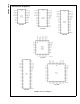
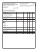
Block Diagram
DS012838-1
FIGURE 1. COP8SAx Block Diagram
COP8SA Family
www.national.com 2