
Datasheet

cui.com
CUI Inc │ SERIES: P7805-S │ DESCRIPTION: NON-ISOLATED SWITCHING REGULATOR date 02/19/2015 │ page 5 of 6
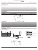
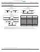
1
3
2
+V
in
GND
-Vou
t
C2
GND
1
2
3
+Vout
C1
C3
C4
LDM
Part Number
C1, C3
(ceramic capacitor)
C2, C4
(ceramic capacitor)
P7805-Q24-S1R5-S 10μF/50V 10μF/6.3V
P7805-Q24-S1R8-S 10μF/50V 10μF/6.3V
P7805-Q24-S2-S 10μF/50V 10μF/6.3V
P7805-Q24-S3-S 10μF/50V 10μF/6.3V
P7805-Q24-S5-S 10μF/50V 10μF/10V
P7805-Q24-S6-S 10μF/50V 10μF/16V
P7805-Q24-S9-S 10μF/50V 10μF/16V
P7805-Q24-S12-S 10μF/50V 10μF/25V
P7805-Q24-S15-S 10μF/50V 10μF/25V
External Capacitor Table
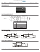
TYPICAL APPLICATION CIRCUIT
Positive Output Application Circuit Negative Output Application Circuit
Positive and Negative Output Paralleling Application Circuit
+V
in
GND
GND
1
2
3
+V
out
C1
C2
+Vin
GND
GND
1
2
3
-Vout
C1
C2
Note: 1. When the products used as negative output and the input-voltage under (Vin-min+2V), C1 and C2 must be added in the circuit, and they should be placed as near as the
products' footprints. Others apply to the application-environment.
2. The capacitance of C1, C2, see external circuit table, can be increased if required, and tantalum or low ESR electrolytic capacitors may also sufce.
3. When the products used as the circuit like gure 4, an inductor named as LDM up to 10μH is recommended in the circuit to reduce the mutual interference.
4. For models ≤ 3.3 V
OUT
, if the input voltage of the model's negative output is less than 4.85 V, a dummy load of not less than 5 mA needs to be added to the output.
5. Cannot use in parallel for output and hot swap for input.
Note: 1. Max. capacitive load tested at input voltage range and full load.
2. All specications measured at: Ta=25°C, humidity<75%, nominal input voltage and rated output load, unless otherwise specied.
Figure 2
Figure 4
Figure 3
For more information, please visit the product page.