
Low Voltage Microcontroller Specification Sheet


CY7C601xx, CY7C602xx
Document 38-16016 Rev. *E Page 37 of 68
16.1.3 P2 Data
16.1.4 P3 Data
16.1.5 P4 Data
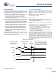
16.2 GPIO Port Configuration
All GPIO configuration registers have common configuration
controls. By default all GPIOs are configured as inputs. To
prevent the inputs from floating, pull up resistors are enabled.
Firmware configures each of the GPIOs before use. The
following are bit definitions of the GPIO configuration registers.
16.2.1 Int Enable
When set, the Int Enable bit allows the GPIO to generate inter-
rupts. Interrupt generate occurs regardless of whether the pin is
configured for input or output. All interrupts are edge sensitive.
However, for interrupts that are shared by multiple sources
(Ports 2, 3, and 4), all inputs are deasserted before a new
interrupt occurs.
When clear, the corresponding interrupt is disabled on the pin.
It is possible to configure GPIOs as outputs, enable the interrupt
on the pin, and then generate the interrupt by driving the appro-
priate pin state. This is useful in test and may find value in appli-
cations as well.
16.2.2 Int Act Low
When clear, the corresponding interrupt is active HIGH. When
set, the interrupt is active LOW. For P0.2–P0.4 Int Act Low
makes interrupts active on the rising edge. Int Act Low set makes
interrupts active on the falling edge.
16.2.3 TTL Thresh
When set, the input has TTL threshold. When clear, the input has
standard CMOS threshold.
Note The GPIOs default to CMOS threshold. User’s firmware
needs to configure the threshold to TTL mode if necessary.
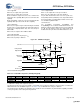
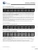
Table 16-3. P2 Data Register (P2DATA) [0x02] [R/W]
Bit # 7 6 5 4 3 2 1 0
Field P2.7–P2.2 P2.1–P2.0
Read/Write R/W R/W R/W R/W R/W R/W R/W R/W
Default 0 0 0 0 0 000
This register contains the data for Port 2. Writing to this register sets the bit values to be output on output enabled pins. Reading
from this register returns the current state of the Port 2 pins.
Bit [7:2]: P2 Data [7:2]
Bit [1:0]: P2 Data [1:0]
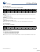
Table 16-4. P3 Data Register (P3DATA) [0x03] [R/W]
Bit # 7 6 5 4 3 2 1 0
Field P3.7–P3.2 P3.1–P3.0
Read/Write R/W R/W R/W R/W R/W R/W R/W R/W
Default 0 0 0 0 0 000
This register contains the data for Port 3. Writing to this register sets the bit values to be output on output enabled pins. Reading
from this register returns the current state of the Port 3 pins.
Bit [7:2]: P3 Data [7:2]
Bit [1:0]: P3 Data [1:0]
Table 16-5. P4 Data Register (P4DATA) [0x04] [R/W]
Bit # 7 6 5 4 3 2 1 0
Field Reserved P4.3–P4.0
Read/Write ––––R/W R/W R/W R/W
Default 00000 0 0 0
This register contains the data for Port 4. Writing to this register sets the bit values to be output on output enabled pins. Reading
from this register returns the current state of the Port 2 pins.
Bit [7:4]: Reserved
Bit [3:0]: P4 Data [3:0]
P4.3–P4.0 only exist in the CY7C601xx.
[+] Feedback [+] Feedback