
Reference Guide
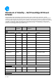
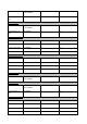
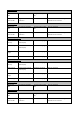

Item
How is data input to this
memory?
How is this memory
write protected?
How is the memory cleared?
Planar
PCH Internal
CMOS RAM
BIOS
N/A – BIOS only
control
1) Set NVRAM_CLR jumper to clear BIOS
configuration settings at boot and
reboot system; 2) AC power off system,
remove coin cell battery for 30 seconds,
replace battery and power back on; 3)
restore default configuration in F2
system setup menu.
BIOS Password
Keyboard
N/A
Place shunt on J_PSWD_NVRAM jumper
pins 2 and 4.
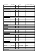
BIOS SPI Flash
SPI interface via iDRAC
Software write
protected
Not possible with any utilities or
applications and system is not functional
if corrupted/removed.
iDRAC SPI Flash
SPI interface via iDRAC
Embedded iDRAC
subsystem firmware
actively controls sub
area based write
protection as needed.
Not completely user clearable; however,
user data, lifecycle log and archive, SEL,
fw image repository can be cleared via
Delete Configuration and Retire System,
accessible in Lifecycle Controller
interface
BMC EMMC
NAND Flash interface via
iDRAC
Embedded FW write
protected
Not completely user clearable; however,
user data, lifecycle log and archive, SEL,
fw image repository can be cleared via
Delete Configuration and Retire System,
accessible in Lifecycle Controller
interface
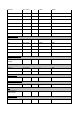
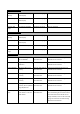
CPU Vcore
Regulators
NA
Not user clearable
Vmem
Regulators
NA
Not user clearable
System CPLD
RAM
Not utilized
Not accessible
Not accessible
System Memory
System OS
OS Control
Reboot or power down system
Internal USB Key
USB interface via PCH.
Accessed via system OS
No write protect
Can be cleared in system OS
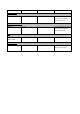
CPU
Various
Various
Power off
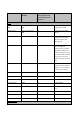
iDRAC DDR
iDRAC Firmware
NA
Power off
iDRAC
iDRAC Firmware
NA
Power off