
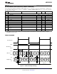
Specifications

ADC12EU050
www.ti.com
SNAS444I –JANUARY 2008–REVISED APRIL 2013
FUNCTIONAL DESCRIPTION
The ADC12EU050 employs a number of unique strategies to provide a high performance multi-channel ADC that
offers a significant power consumption reduction when compared to compteting architectures, as well as easing
system level design. The ultra-low power performance of the ADC12EU050 is derived from the implementation of
a fast continuous time sigma delta (CT∑Δ) modulator. Other features of this technology are:
• Intrinsic anti-alias filter – the digital decimating filter provides an intrinsic anti-alias filter, eliminating external
analog filter components, and simplifying multi-channel designs.
• Instant overload recovery (IOR) system ensures extremely fast recovery from overload (<1ps), and no settling
errors on return from overload.
• Ultra-low inter-channel crosstalk.
• Digital Equalizer provides low group delay and hence minimizes signal path delay variation.
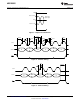
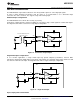
The major signal path blocks are: clipping control; CT∑Δ modulator; digital decimation filter; 12 bit serializer; and
finally the LVDS/SLVS outputs. The PLL is critical to the operation of the ADC12EU050, and the PLL also
provides the bit and word clock outputs. The SPI Control Interface gives uncomplicated user access to the ADC
registers.
12-BIT SIGMA DELTA ADC CORE
The ADC12EU050 comprises eight analog ADC channels using a CT∑Δ architecture, which provides very high
dynamic performance with ultra-low power, while operating from a minimal 1.2V supply.
The CT∑Δ ADC architecture uses a third order sigma delta modulator operating at a nominal 16 times over-
sampling rate in combination with a 3-bit quantizer. The modulator output is coupled to a power efficient digital
decimation filter that decimates the high rate modulator output (720MHz) to provide output data at a 45 MSPS
sample rate.
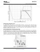
A benefit of the CT∑Δ design is that the ADC requires no external anti-alias filters for most applications. This
benefit is derived from a combination of the design of the analog sigma delta modulator and digital decimation
filter. The digital filter achieves a steep transition band, and provides 72 dB of attenuation in the stop band. Using
the digital equalizer, the signal transfer characteristics including phase performance can be optimized so as to
minimise group delay variation. In applications where it is not required, the digital equalizer can be disabled to
further save power.
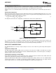
DIFFERENTIAL INPUT STAGE
The ADC can capture high speed analog signals without resorting to a complex fast sample-and-hold amplifier
(SHA) as used in pipeline ADCs. This is where CT∑Δ technology derives much of its power and performance
benefits. This feature also assists external circuit design. In the case of the SHA inputs of pipeline ADCs, the
effective input capacitance is time variant, requiring a powerful input buffer to drive to the resolution limits of the
system. The input stage of the ADC is purely resistive (1.3kΩ single ended) driving into virtual earth. As a result
the ADC12EU050 is extremely easy to drive as its input impedance is not complex. It also means that external
lower power input buffering circuitry can used, and can be completely eliminated in some cases.
Copyright © 2008–2013, Texas Instruments Incorporated Submit Documentation Feedback 13
Product Folder Links: ADC12EU050