
Specifications

-80
-60
-40
-20
0
GAIN (dB)
10
1
10
2
10
3
10
4
10
5
OFFSET (Hz)
20
40
10
6
10
7
10
8
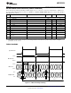
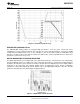
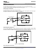
Loop Bandwidth at 0.415 MHz
Loop Bandwidth at 1.50 MHz
-80
-60
-40
-20
0
GAIN (dB)
10
1
10
2
10
3
10
4
10
5
OFFSET (Hz)
20
40
10
6
10
7
10
8
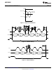
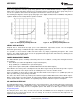
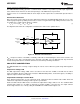
Loop Bandwidth at 0.380 MHz
Loop Bandwidth at 1.280 MHz
ADC12EU050
SNAS444I –JANUARY 2008–REVISED APRIL 2013
www.ti.com
CLOCK SELECTION CONSIDERATIONS
The ADC12EU050 has an on-chip PLL, which simplifies the task of clock source selection and clock network
design.
Clock Input Connection
The ADC is designed to accept either single ended or differential clock inputs. Furthermore, the clock source can
be a sine or square wave. In order to obtain the best performance, a differential square wave clock should be
used. When using a differential clock, the clock traces should be routed as 100Ω differential pairs, and
terminated with a 100Ω resistor close to the chip. A single ended clock input should be connected to pin 47
(CLK+/SE), and pin 48 (CLK-) should be grounded.
On-chip PLL
The benefit of having an on chip PLL is that in most applications a high precision clock source is not required.
The external clock's contribution to aperture jitter is reduced dramatically by the jitter clean-up properties of the
PLL, which ensures that any RMS jitter outside of the PLL bandwidth is attenuated. The PLL also significantly
relaxes the input clock duty cycle requirements, accepting input clock duty cycles of 20% to 80%.
The PLL offers two choices of bandwidth. For the majority of systems, the default bandwidth of 400kHz is
suitable. If the system already contains a high performance clock, with excellent RMS jitter performance up to a
1.4MHz bandwidth, then the PLL’s high bandwidth mode may be used.
Figure 12. PLL Phase Noise Transfer Function: f
s
= Figure 13. PLL Phase Noise Transfer Function: f
s
=
40MHz 50MHz
On the input clock, excessive RMS jitter within the PLL bandwidth will be seen in the output spectrum as
sidebands, or close in phase noise, around the fundamental signal.
Input Clock Selection
For systems which do not have a requirement for a high performance clock, any standard product 45MHz crystal
oscillator will allow the ADC12EU050 to perform to specifications. If the system requires high performance clocks
for other system components, then Texas Instruments' LMK family of clock conditioners are recommended.
Output Clock Synchronization Across Multiple Chips
In systems containing more than one ADC12EU050, it is often required that the timing of output samples is
synchronized across the multiple chips. The PLL in the ADC12EU050 takes care of this automatically by aligning
the output clocks with the input clock. The user must ensure, using correct board layout and clock buffering
techniques, that the input clock to each ADC12EU050 is synchronized. If this is the case, then the output frame
clocks will also be synchronized. This means that output samples are aligned.
18 Submit Documentation Feedback Copyright © 2008–2013, Texas Instruments Incorporated
Product Folder Links: ADC12EU050