
Data Sheet

LT3652
10
3652fe
For more information www.linear.com/LT3652
APPLICATIONS INFORMATION
Overview
LT3652 is a complete monolithic, mid-power, multi-chem
-
istry buck battery charger, addressing high input voltage
applications with solutions that require a minimum of exter
-
nal components. The IC uses a 1MHz constant frequency,
average-current mode step-down architecture.
The LT3652 incorporates a 2A switch that is driven by
a bootstrapped supply to maximize efficiency during
charging cycles. Wide input range allows operation to full
charge from voltages as high as 32V. A precision threshold
shutdown pin allows incorporation of UVLO functionality
using a simple resistor divider. The IC can also be put into
a low-current shutdown mode, in which the input supply
bias is reduced to only 15µA.
The LT3652 employs an input voltage regulation loop,
which reduces charge current if a monitored input volt
-
age falls below a programmed level. When the LT3652 is
powered by a solar panel, the input regulation loop is used
to maintain the panel at peak output power.
The LT3652 automatically enters a battery precondition
mode if the sensed battery voltage is very low. In this mode,
the charge current is reduced to 15% of the programmed
maximum, as set by the inductor sense resistor, R
SENSE
.
Once the battery voltage reaches 70% of the fully charged
float voltage, the IC automatically increases maximum
charge current to the full programmed value.
The LT3652 can use a charge-current based C/10 termina
-
tion scheme, which ends a charge cycle when the battery
charge current falls to one tenth of the programmed
maximum charge current. The LT3652 also contains an
internal charge cycle control timer, for timer-based termina
-
tion. When using the internal timer, the IC combines C/10
detection with a programmable time constraint, during
which the charging cycle can continue beyond the C/10
level to top-off a battery. The charge cycle terminates
when a specific time elapses, typically 3 hours. When
the timer-based scheme is used, the IC also supports bad
battery detection, which triggers a system fault if a battery
stays in precondition mode for more than one eighth of
the total charge cycle time.
Once charging is terminated, the LT3652 automatically
enters a low-current standby mode where supply bias
currents are reduced to 85µA. The IC continues to monitor
the battery voltage while in standby, and if that voltage
falls 2.5% from the full-charge float voltage, the LT3652
engages an automatic charge cycle restart. The IC also
automatically restarts a new charge cycle after a bad bat
-
tery fault once the failed battery is removed and replaced
with another battery.
The LT3652 contains provisions for a battery temperature
monitoring circuit. This feature monitors battery tempera
-
ture using a thermistor during the charging cycle. If the
battery temperature moves outside a safe charging range
of 0°C to 40°C, the IC suspends charging and signals a
fault condition until the temperature returns to the safe
charging range.
The LT3652 contains two digital open-collector outputs,
which provide charger status and signal fault conditions.
These binary-coded pins signal battery charging, standby
or shutdown modes, battery temperature faults, and bad
battery faults.
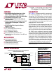
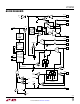
General Operation (See Block Diagram)
The LT3652 uses average current mode control loop
architecture, such that the IC servos directly to average
charge current. The LT3652 senses charger output voltage
through a resistor divider via the V
FB
pin. The difference
between the voltage on this pin and an internal 3.3V volt
-
age reference is integrated by the voltage error amplifier
(V-EA). This amplifier generates an error voltage on its
output (I
TH
), which corresponds to the average current
sensed across the inductor current sense resistor, R
SENSE
,
which is connected between the SENSE and BAT pins.
The I
TH
voltage is then divided down by a factor of 10,
and imposed on the input of the current error amplifier
(C-EA). The difference between this imposed voltage and
the current sense resistor voltage is integrated, with the
resulting voltage (V
C
) used as a threshold that is compared
against an internally generated ramp. The output of this
comparison controls the charger’s switch.