
Data Sheet
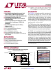

LT3652
8
3652fe
For more information www.linear.com/LT3652
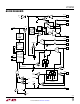
NTC (Pin 8): Battery Temperature Monitor Pin. This pin is
the input to the NTC (Negative Temperature Coefficient)
thermistor temperature monitoring circuit. This function is
enabled by connecting a 10kΩ, B = 3380 NTC thermistor
from the NTC pin to ground. The pin sources 50µA, and
monitors the voltage across the 10kΩ thermistor. When
the voltage on this pin is above 1.36 (T < 0°C) or below
0.29V (T > 40°C), charging is disabled and the CHRG and
FA U LT pins are both pulled low. If internal timer termina
-
tion is being used, the timer is paused, suspending the
charging cycle. Charging resumes when the voltage on NTC
returns to within the 0.29V to 1.36V active region. There
is approximately 5°C of temperature hysteresis associated
with each of the temperature thresholds. The temperature
monitoring function remains enabled while the thermistor
resistance to ground is less than 250k, so if this function
is not desired, leave the NTC pin unconnected.
BAT (Pin 9): Charger Output Monitor Pin. Connect a
10µF decoupling capacitance (C
BAT
) to ground. Depend-
ing on application requirements, larger value decoupling
capacitors may be required. The charge function operates
to achieve the programmed output battery float voltage
(V
BAT(FLT)
) at this pin. This pin is also the reference for
the current sense voltage. Once a charge cycle is termi
-
nated, the input bias current of the BAT pin is reduced to
< 0.1µA, to minimize battery discharge while the charger
remains connected.
SENSE (Pin 10): Charge Current Sense Pin. Connect the
inductor sense resistor (R
SENSE
) from the SENSE pin to the
BAT pin. The voltage across this resistor sets the average
charge current. The maximum charge current (I
CHG(MAX)
)
corresponds to 100mV across the sense resistor. This
resistor can be set to program maximum charge cur
-
rent as high as 2A. The sense resistor value follows the
relation:
R
SENSE
= 0.1/I
CHG(MAX)
(Ω)
Once a charge cycle is terminated, the input bias current of
the SENSE pin is reduced to < 0.1µA, to minimize battery
discharge while the charger remains connected.
BOOST (Pin 11): Bootstrapped Supply Rail for Switch
Drive. This pin facilitates saturation of the switch transistor.
Connect a 1µF or greater capacitor from the BOOST pin
to the SW pin. Operating range of this pin is 0V to 8.5V,
referenced to the SW pin. The voltage on the decoupling
capacitor is refreshed through a rectifying diode, with
the anode connected to either the battery output voltage
or an external source, and the cathode connected to the
BOOST pin.
SW (Pin 12): Switch Output Pin. This pin is the output
of the charger switch, and corresponds to the emitter of
the switch transistor. When enabled, the switch shorts
the SW pin to the V
IN
supply. The drive circuitry for this
switch is bootstrapped above the V
IN
supply using the
BOOST supply pin, allowing saturation of the switch for
maximum efficiency. The effective on-resistance of the
boosted switch is 0.175Ω.
GND (Pin 13): Ground Reference and Backside Exposed
Lead Frame Thermal Connection. Solder the exposed lead
frame to the PCB ground plane.
PIN FUNCTIONS