250 DIAMOND-MM-48-AT Autocalibrating 16-bit Analog I/O PC/104 Module With Relays and Optocouplers User Manual V1.01 Copyright 2004 Diamond Systems Corporation 8430-D Central Ave. Newark, CA 94560 Tel (510) 456-7800 www.diamondsystems.
TABLE OF CONTENTS 1. DESCRIPTION.......................................................................................................................... 3 2. DIAMOND-MM-48-AT BOARD DRAWING ............................................................................. 4 3. I/O HEADER PINOUT AND PIN DESCRIPTION..................................................................... 5 4. BOARD CONFIGURATION ..................................................................................................
DIAMOND-MM-48-AT Autocalibrating Analog I/O PC/104 Module 1. DESCRIPTION Diamond-MM-48-AT (DMM-48-AT) is a PC/104 expansion board offering embedded systems designers a full feature set of analog and digital I/O capabilities. It is designed to be used in any PC-compatible embedded computer with a PC/104 (ISA-bus) expansion connector. DMM-48-AT offers reduced embedded system size and weight, as well as lower cost, by providing more functionality on one board than other data acquisition boards.
2. DIAMOND-MM-48-AT BOARD DRAWING Feature descriptions J1 PC/104 8-bit bus connector J2 PC/104 16-bit bus connector J3 Analog and digital I/O connector J4 Relay and optocoupler I/O connector J6 Configuration jumper block J7 Factory use only (used in factory calibration process) J10 +/-5 input range selection (bipolar model only) Diamond-MM-48-AT User Manual V1.
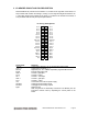
3. I/O HEADER PINOUT AND PIN DESCRIPTION Diamond-MM-48-AT provides two I/O headers. J3, located on the right side of the board, is a 40-pin header that includes the analog in, analog out, and logic-level digital I/O features. Pin 1 is the upper left pin and is marked on the board. J4, located on the left side of the baord, is a 34-pin header with the relay and optocoupler features.
J4: Relays and Optocouplers Opto 0Opto 1Opto 2Opto 3No connection Relay 0 NO Relay 0 C Relay 1 NC Relay 2 NO Relay 2 C Relay 3 NC Relay 4 NO Relay 4 C Relay 5 NC Relay 6 NO Relay 6 C Relay 7 NC Signal Name 1 3 5 7 9 11 13 15 17 19 21 23 25 27 29 31 33 2 4 6 8 10 12 14 16 18 20 22 24 26 28 30 32 34 Opto 0+ Opto 1+ Opto 2+ Opto 3+ No connection Relay 0 NC Relay 1 NO Relay 1 C Relay 2 NC Relay 3 NO Relay 3 C Relay 4 NC Relay 5 NO Relay 5 C Relay 6 NC Relay 7 NO Relay 7 C Definition Relay output contacts:
4. BOARD CONFIGURATION Refer to the Drawing of Diamond-MM-48-AT on page 4 for locations of the configuration items mentioned here. All configuration except the A/D input range is done with jumper block J6. 4.1 Base Address Each board in your system must have a unique I/O address range. The first address in this range is called the base address. Diamond-MM-48-AT uses an I/O range of 16 bytes.
board should have the pull-down resistor enabled with a jumper in the R location. The other boards should have the R jumper removed to disable their pull-down resistors. 4.3 Optocoupler Polarity The 4 optocouplers may be configured for either direct or inverted polarity with the POL position on J6. For direct polarity, an open circuit / low voltage input reads back as a 0, and a high voltage reads back as a 1. For inverted polarity, an open circuit / low voltage reads as 1, and a high voltage reads as 0.
5. I/O MAP 5.1 Overview Diamond-MM-48-AT occupies 16 bytes in I/O memory space. A functional list of these registers is provided below, and detailed register bit definitions are provided on the next page and the following chapter. The information in chapters 5 and 6 is provided to assist in understanding the board’s operation and for use by programmers writing their own driver software.
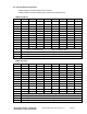
5.2 Register Map Bit Assignments A blank location in the Write registers has no function. A blank location in the Read registers has no function and reads back as 0.
6. REGISTER DEFINITIONS Base + 0 Write D/A LSB Bit No. 7 6 5 4 3 2 1 0 Name DA7 DA6 DA5 DA4 DA3 DA2 DA1 DA0 Definitions: DA7-0 Base + 0 D/A bits 7-0; DA0 is the LSB. D/A data is an unsigned 12-bit number ranging from 0 to 4095. Read A/D LSB Bit No. 7 6 5 4 3 2 1 0 Name AD7 AD6 AD5 AD4 AD3 AD2 AD1 AD0 Definitions: AD7 – 0 Base + 1 A/D LSB data (bits 7-0 of the 16-bit value). A/D data is a signed 16-bit value ranging from -32768 to 32767. Write Bit No.
Base + 1 Read A/D MSB Bit No. 7 6 5 4 3 2 1 0 Name AD15 AD14 AD13 AD12 AD11 AD10 AD9 AD8 Definitions: AD15 – 8 A/D MSB data (bits 15-8 of the 16-bit value). A/D data is a signed 16-bit value ranging from -32768 to 32767. Note: Reading from Base + 0 and Base + 1 result in the same physical operation, reading from the FIFO. The FIFO is 8 bits wide x 2048 bytes deep, with A/D data stored and retrieved in interleaved fashion.
Base + 3 Read/Write Relay Control Port Bit No. 7 6 5 4 3 2 1 0 Name RELAY7 RELAY6 RELAY5 RELAY4 RELAY3 RELAY2 RELAY1 RELAY0 These bits control the 8 relays. 0 = off (C connected to NC), 1 = on (C connected to NO). The written value may be read back with true logic. The value on the corresponding output pin is the inverse of the value in this register.
Base + 5 Write Bit No. Digital I/O Data 7 6 5 4 Name 3 2 1 0 DIO3 DIO2 DIO1 DIO0 Definitions: DIO3 – 0 Base + 5 Digital I/O output data. Only bits in output mode are affected. Any bit in input mode will ignore data written to this register. Read Bit No.
Base + 7 Write Bit No. 7 D/A Channel and Control Register 6 5 4 Name DAUPDT 3 2 1 0 DAUPDT DACH2 DACH1 DACH0 Writing a 1 to this bit updates the D/A chip. All channels with new data written to them since the previous update are updated simultaneously. When a 1 is written to this bit the other bits in the register are ignored. When DAUPDT = 0, the remaining bits in this register behave as described below: DACH2-0 Base + 7 Read Bit No.
Base + 8 Bit No. Write 7 Command Register 6 5 Name 4 3 2 DAPRE DAPRLD RESET 1 0 FIFORST ADSTART Writing a 1 to any bit in this register causes a command or operation to be executed. Only one bit may be activated (set to 1) at a time. When a 1 is written to any bit, no other bit or related operation is affected. DAPRE All 8 D/A channels are set to the value in the D/A preset register. This value is user-definable and can be used for any purpose.
Base + 8 Bit No. Name POL Read 7 Status Register 6 5 4 3 2 1 0 POL ADCH3 ADCH2 ADCH1 ADCH0 Optocoupler polarity jumper setting; the value indicates the value of an open circuit: 1 Open circuit reads as 1, “high” input reads as 0 0 Open circuit reads as 0, “high” input reads as 1 ADCH3 - 0 Current A/D channel; this is the channel currently selected on board and is the channel that will be used for the next A/D conversion (unless a new value is written to the channel register before then).
Base + 9 Bit No. Name Write 7 Configuration Register 6 5 CKSEL1 4 3 CKFRQ1 CKFRQ0 2 1 0 SCNINT CLKEN CLKSEL CKSEL1 Clock source select for counter/timer 1: 1 External signal Clk0 in I/O connector J3 0 On-board clock, frequency selected by CKFRQ1 below CKFRQ1 Clock frequency select for counter/timer 1 when CKSEL1 = 0: 1 100KHz 0 10MHz CKFRQ0 Clock frequency select for counter/timer 0: 1 1MHz 0 10MHz SCNINT Scan interval. This is the time between A/D samples during an A/D scan.
Base + 9 Read Bit No. Name 7 Configuration & Status Register 6 ADBUSY DABUSY ADBUSY 5 CKSEL1 4 3 CKFRQ1 CKFRQ0 2 1 0 SCNINT CLKEN CLKSEL A/D chip status: 1 A/D conversion or scan is in progress or A/D input circuit in settling mode 0 A/D is idle Do not attempt to start a new A/D conversion or scan when ADBUSY = 1. DABUSY D/A chip status: 1 D/A conversion is in progress 0 D/A is idle Do not attempt to start a new D/A conversion when DABUSY = 1.
Base + 10 Bit No. Write 7 FIFO Control Register 6 5 4 Name 3 2 1 0 PAGE FIFOTH FIFOEN SCANEN PAGE Page number for registers at Base + 12 through Base + 15 Page 0: 82C54 counter/timer access Page 1: Calibration registers FIFOTH FIFO threshold: 0 = 1024 samples (half full), 1 = 256 samples (1/8 full) FIFOEN FIFO enable: 1 Enable FIFO operation; if interrupts are enabled, interrupt requests will occur when the FIFO reaches or exceeds the threshold selected with FIFOTH.
Base + 11 Write Interrupt Control Register Bit No. 7 6 5 4 3 2 1 0 Name CLRT CLRD CLRO CLRA TINTE DINTE OINTE AINTE CLRT Clear the timer interrupt flip flop. CLRD Clear the digital input interrupt flip flop and reset their edge detect status bits. CLRO Clear the optocoupler input interrupt flip flop and reset their edge detect status bits. CLRA Clear the analog input interrupt flip flop.
Base + 11 Read Interrupt Status Register Bit No.
Page 0: Counter/Timer Base + 12 Read/Write Counter/Timer D7 - 0 Bit No. 7 6 5 4 3 2 1 0 Name D7 D6 D5 D4 D3 D2 D1 D0 This register is used for both Counter 0 and Counter 1. It is the LSB for both counters. When writing to this register, an internal load register is loaded. Upon issuing a Load command through Base + 15, the selected counter’s LSB register will be loaded with this value. When reading from this register, the LSB value of the most recent Latch command will be returned.
Base + 15 Write Counter/Timer Control Register Bit No. 7 6 5 4 3 2 1 0 Name CTRNO LATCH GTDIS GTEN CTDIS CTEN LOAD CLR This register is used to control the counter/timers. A counter is selected with bit 7, and then a 1 is written to any ONE of bits 6 – 0 to select the desired operation for that counter. The other bits and associated functions are not affected. Thus only one operation can be performed at a time. CTRNO Counter no.
Page 1: Autocalibration Control Registers Base + 12 Read/Write EEPROM / TrimDAC Data Register Bit No. 7 6 5 4 3 2 1 0 Name D7 D6 D5 D4 D3 D2 D1 D0 D7-0 Calibration data to be read or written to the EEPROM and/or TrimDAC. During EEPROM or TrimDAC write operations, the data written to this register will be written to the selected device. During EEPROM read operations this register contains the data to be read from the EEPROM and is valid after EEBUSY = 0 (Page 1, Base + 14).
Base + 14 Write Calibration Control Register Bit No. 7 6 5 Name EE_EN EE_RW 4 3 2 1 0 RUNCAL CMUXEN TDACEN This register is used to initiate various commands related to autocalibration. More detailed information on autocalibration may be found elsewhere in this manual. EE_EN EEPROM Enable. Writing a 1 to this bit will initiate a transfer to/from the EEPROM as indicated by the EE_RW bit. EE_RW Selects read or write operation for the EEPROM: 0 = Write, 1 = Read.
7. ANALOG INPUT RANGES AND RESOLUTION 7.1 Resolution Diamond-MM-48-AT uses a 16-bit A/D converter. This means that the analog input voltage can be measured to the precision of a 16-bit binary number. The maximum value of a 16-bit binary number is 216 - 1, or 65535, so the full range of numerical values that you can get from a Diamond-MM-48-AT analog input channel is 0 - 65535. The smallest change in input voltage that can be detected is 1/(216), or 1/65536, of the fullscale input range.
8. PERFORMING AN A/D CONVERSION This chapter describes the steps involved in performing an A/D conversion on a selected input channel using direct programming (not with the driver software). This describes the basic operation of a single A/D conversion without interrupts. For a more complete description including interrupts and all register control bits, see chapter 9. There are five steps involved in performing an A/D conversion: 1. Select the input channel 2. Wait for analog input circuit to settle 3.
8.3 Trigger an A/D conversion on the current channel After the above steps are completed, start the A/D conversion by writing a 1 to the ADSTART bit in Base + 8. This write operation only triggers the A/D if the CLKEN bit is 0 to disable hardware triggering and enable software triggering. Otherwise the A/D will only trigger when the selected clock or trigger signal occurs. CLKEN should always be 0 when controlling A/D conversions in software. 8.
8.6 Convert the numerical data to a meaningful value Once you have the A/D code, you need to convert it to a meaningful value. The first step is to convert it back to the actual measured voltage. Afterwards you may need to convert the voltage to some other engineering units (for example, the voltage may come from a temperature sensor, and then you would need to convert the voltage to the corresponding temperature according to the temperature sensor’s characteristics).
9. A/D SCAN, FIFO, AND INTERRUPT OPERATION This chapter describes in detail the interrupt performance of the A/D circuit under all conditions. The control bits FIFOEN (FIFO enable), FIFOTH (FIFO threshold), SCANEN (scan enable), SCNINT (scan interval), and AINTE (A/D interrupt enable) determine the behavior of the board during A/D conversions with interrupts. Control bits CLKEN and CLKSEL determine the source of the A/D trigger, either software, on-board counter/timer, or external signal.
FIFO Operation After each A/D conversion is completed, the A/D data is stored in the FIFO. The data is inserted in LSB / MSB sequence. The FIFO holds 4096 bytes, or 2048 samples. It has several flags that indicate its state: EF Empty flag 1 when the FIFO is empty and 0 otherwise.
Guidelines for Selecting FIFO Use (FIFOEN and FIFOTH) The below data is a guideline for interrupt use that will work in typical applications and systems. Each application’s optimum performance will be based on the processor speed, operating system, sampling method, and need to obtain data as soon as possible. Sample rate Suggested use Rate < 500Hz FIFO not needed; one interrupt per sample or scan is acceptable. This setting applies to both single A/D samples and A/D scans.
10. ANALOG OUTPUT OVERVIEW 10.1 Description Diamond-MM-48-AT uses an 8-channel 12-bit D/A converter (DAC) to provide 8 analog voltage outputs. A 12-bit DAC can generate output voltages with the precision of a 12-bit binary number. The maximum value of a 12-bit binary number is 212 - 1, or 4095, so the full range of numerical values that you can write to the analog outputs on Diamond-MM-48-AT is 0 - 4095.
11. GENERATING AN ANALOG OUTPUT This chapter describes the steps involved in generating an analog output (also called performing a D/A conversion) on a selected output channel using direct programming (not with the driver software). There are three steps involved in performing a D/A conversion: 1. Compute the D/A code for the desired output voltage 2. Write the value to the selected output channel 3. Update the D/A 11.
12. AUTOCALIBRATION OPERATION Diamond-MM-48-AT includes a sophisticated autocalibration circuit that manages the calibration of both the A/D and the D/A circuitry. Operation is as follows. 12.1 Reference Voltages The board contains a precision reference voltage chip that is selected for high stability over time and temperature. The value of the voltage output from this chip is measured at the factory.
13. DIGITAL I/O OPERATION Diamond-MM-48-AT contains a 4-bit digital I/O port with programmable direction and edge detection capability. The digital I/O lines are located at pins 35 through 38 on the I/O header J3. They are CMOS / TTL compatible. Each line can drive up to -6mA in a logic high state or sink up to 8mA in a logic low state. All digital input lines have 10KΩ pull-up resistors. The I/O lines are written and read with 4 bits in the register at Base + 5.
14. OPTOCOUPLER OPERATION Diamond-MM-48-AT contains 4 optocoupler inputs with programmable polarity, programmable edge detection capability, and interrupt capability on edge detection. These lines accept inputs up to 28VDC. The transition between logic 0 and 1 occurs at approximately 1.5VDC and is guaranteed to be 1 at 3VDC or above. The POL jumper on jumper block J6 selects the logic polarity of the 4 register bits OPTO3-0. The POL jumper can be read with the POL bit in Base + 8.
Tables describing behavior of POL jumper, opto inputs, and edge detection The POL bit is the inverse of the POL pin. Non-inverted inputs means the opto bit is reported as the inverse of the corresponding input pin, since the opto circuit has a built-in inversion. Edge detection always operates with respect to the actual input voltage, not the logic. Rising always means from 0V to 3V, and falling always means from 3V to 0V. 1.
15. RELAY OPERATION Diamond-MM-48-AT contains 8 relays with SPDT (form C) configuration. The relays are Omron type G6K or equivalent. Note that these relays are actually DPDT (double pole) relays. The two poles are connected in parallel for lower on resistance and greater current carrying capacity.
16. COUNTER/TIMER OPERATION Diamond-MM-48-AT contains two counter/timers that provide various timing functions, including A/D timing and user functions. These counters are integrated into the system controller FPGA. The user interface consists of a 24-bit data register in Base + 12 through Base + 14, an 8-bit command register in Base + 15, and control bits in several other registers.
16.3 Command Sequences Diamond Systems provides Universal Driver software to control the counter/timers on Diamond-MM-48-AT. The information here is intended as a guide for programmers writing their own code in place of the driver and also to give a better understanding of the counter/timer operation. The counter control register is shown below. Base + 15 Write Counter/Timer Control Register Bit No.
Reading a counter a. Latch the counter: Counter 0 outp(base+15,0x40); Counter 1 outp(base+15,0xC0); b. Read the data: The value is returned in 3 bytes, low, middle, and high (2 bytes for counter 1) Counter 0 low=inp(base+12); middle=inp(base+13); high=inp(base+14); c.
17. SPECIFICATIONS Analog Inputs No.