
Datasheet


1300 Henley Court
Pullman, WA 99163
509.334.6306
www.digilentinc.com
JTAG-HS3™ Programming Cable for Xilinx
®
FPGAs
Revised June 30, 2014
This manual applies to the JTAG-HS3 rev. A
DOC#: 502-299
Copyright Digilent, Inc. All rights reserved.
Other product and company names mentioned may be trademarks of their respective owners.
Page 1 of 6
Overview
The JTAG-HS3 programming cable is a high-speed programming/debugging solution for Xilinx FPGAs and SoCs. It is
fully compatible will all Xilinx Tools, and can be seamlessly driven from iMPACT, ChipScope™, EDK, and Vivado™.
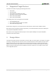
The HS3 attaches to target boards using Xilinx’s 2x7, 2mm programming header.
The PC powers the JTAG-HS3 through the USB port and will recognize it as a Digilent programming cable when
connected, even if the cable is not attached to the target board. The HS3 has a separate Vref pin to supply the
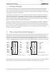
JTAG signal buffers. The high speed 24mA three-state buffers allow the HS3 to drive target boards with signal
voltages from 1.8V to 5V and bus speeds up to 30MBit/sec (see Fig. 1). To function correctly, the HS3’s Vref pin
must be tied to the same voltage supply (VCCO_0) that drives the JTAG port on the FPGA.
The JTAG bus can be shared with other devices as the HS3 signals are held in high-impedance, except when
actively driven during programming. The HS3 uses a standard Type-A to Micro-USB cable that attaches to the end
of the module opposite the system board connector. The HS3 is small and light, allowing it to be held firmly in
place by the system board connector (see Fig. 2).
The JTAG-HS3
Small, complete, all-in-one JTAG
programming/debugging solution for Xilinx FPGAs and
SoCs
Plugs directly into standard Xilinx JTAG header
Separate Vref drives JTAG signal voltages; Vref can be
any voltage between 1.8V and 5V
High-Speed USB2 port that can drive JTAG bus up to
30Mbit/sec (frequency adjustable by user)
Compatible with Xilinx ISE® 14.1 and newer, Xilinx
Vivado 2013.3 and newer
Uses micro_AB USB2 connector
Open drain buffer on pin 14 allows debugging software
to reset the processor core of Xilinx’s Zynq® platform
Figure 2. Xilinx JTAG header. Dual row, 2mm, 14 pin.
Figure 1. Diagram of signal voltages and connections.
V
IO
: 5V to 1.8V
USB2
Port
TMS
TDI
TDO
TCK
TMS
TDI
TDO
TCK
FPGAJTAG-HS3
GND
VREF
GND
VIO
Features include: