
Datasheet


JTAG-HS3™ Reference Manual
Copyright Digilent, Inc. All rights reserved.
Other product and company names mentioned may be trademarks of their respective owners.
Page 2 of 6
1 Software Support
The JTAG-HS3 has been designed to work seamlessly with Xilinx’s ISE (iMPACT, ChipScope, EDK) and Vivado tool
suites. The most recent versions of ISE and Vivado include all of the drivers, libraries, and plugins necessary to
communicate with the JTAG-HS3. At the time of writing, the following Xilinx software included support for the HS3:
Vivado 2014.1+, Vivado 2013.3+, and ISE 14.1+.
The HS3 is also compatible with ISE 13.1 – 13.4. However, these versions of ISE do not include all of the libraries,
drivers, and plugins necessary to communicate with the HS3. In order to use the JTAG-HS3 with these versions of
ISE, version 2.5.2 or higher of the Digilent Plugin for Xilinx Tools package must be downloaded from the Digilent
website, and the ISE13 plugin must be manually installed as described in the included documentation. The JTAG-
HS3 is not compatible with Xilinx Vivado 2013.1 or Vivado 2013.2.
In addition to working with the Xilinx Tools, the HS3 is also supported by Digilent’s Adept software and the Adept
SDK (the SDK is available to download free from Digilent’s website). Adept includes a full-featured programming
environment and a set of public APIs that allow user applications to directly drive the JTAG chain. Using the Adept
SDK, custom applications can be created to drive JTAG ports on virtually any device. Please see the Adept SDK
reference manual for more information.
2 Xilinx Zynq-7000 and SoC Support
The Xilinx Tools occasionally require the processor core of the Zynq-7000 to be reset during debug operations. The
Zynq platform processor has a pin dedicated for this purpose (PS_SRST_B). Driving the PS_SRST_B pin low causes
the processor to reset while maintaining any existing break points and watch points. The JTAG-HS3 is capable of
driving this pin low under the instruction of Xilinx’s SDK during debugging operations. In order for this to work, pin
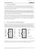
14 of Xilinx JTAG header on the target board must be connected to the PS_SRST_B pin of the Zynq (see Figs. 3 & 4).
1
3
5
7
9
11
13
2
4
6
8
10
12
14
GND
GND
GND
GND
GND
GND
GND
VREF
TMS
TCK
TDO
TDI
----
SRST
1
3
5
7
9
11
13
2
4
6
8
10
12
14
GND
GND
GND
GND
GND
GND
GND
VCCO_0
TMS
TCK
TDO
TDI
----
PS_SRST_B
The JTAG-HS3 uses an open drain buffer to drive pin 14 of the Xilinx JTAG header (see Fig. 5). This allows the HS3 to
drive the PS_SRST_B pin when VCC_MIO1 is referenced to a different voltage than VCCO_0 (see Fig. 6).
Figure 3. JTAG-HS3 pinout (seen looking out of the connector).
Figure 4. Xilinx System Board Header (seen looking into the connector).