
Datasheet


JTAG-HS3™ Reference Manual
Copyright Digilent, Inc. All rights reserved.
Other product and company names mentioned may be trademarks of their respective owners.
Page 3 of 6
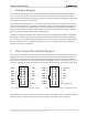
Output Pin
(SRST)
100
Should an accidental short occur between pin 14 and GND, the 100 ohm series resistor protects the buffer from
being damaged. While this resistor protects the buffer from being damaged, it also limits the drive strength of the
buffer. Therefore, it is necessary for the pull-up resistor (R
PU
) used to establish the voltage level on PS_SRST_B to
be greater than or equal to 1.5K ohms. At the time of writing, Xilinx ZC702, Xilinx ZC706, and Avnet® MicroZed™ all
feature 10K pull-ups on pin 14 of the their respective Xilinx JTAG headers. For compatibility with other evaluation
platforms, please consult the manufacturer’s schematic.
Optional Reset
Button
VCCO_0
VCCO_MIO1
PS_SRST_B
ZYNQ-7000
TDO
TMS
TDI
TCK
GND
VREF
TDO
JTAG-HS3
GND
TMS
TDI
TCK
SRST
VCCO_0
VCCO_MIO1
VCCO_MIO1
≥1.5K
R
PU
Figure 5. JTAG-HS3 pin 14 output buffer.
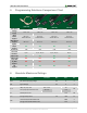
Figure 6.
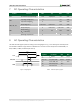
Figure 6. System board components.