
Datasheet


JTAG-HS3™ Reference Manual
Copyright Digilent, Inc. All rights reserved.
Other product and company names mentioned may be trademarks of their respective owners.
Page 6 of 6
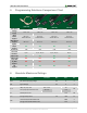
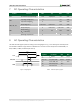
7 DC Operating Characteristics
Symbol
Parameter
Min
Typ
Max
Unit
Vref
I/O reference/supply voltage
1.65
1.8/2.5/3.3
5.5
Volts
TDO
Input High Voltage (V
IH
)
1.4
5.5
Volts
Input Low Voltage (V
IL
)
0
0.45
Volts
TMS, TCK, TDI
Output High (V
OH
)
0.75 x Vref
0.90 x Vref
Vref
Volts
Output Low (V
OL
)
0
0.05 x Vref
0.15 x Vref
Volts
SRST
Output Low (V
OL
)
(R
PU
= 1.5K ohm)
0
0.4
0.55
Volts
T
A
Operating Temperature
0
70
ºC
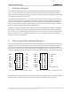
8 AC Operating Characteristics
The JTAG-HS3 JTAG signals operate according to the timing diagram in Fig. 7. The HS3 supports TCK frequencies
from 30 MHz to 8 KHz at integer divisions of 30 MHz from 1 to 3750. Common frequencies include 30 MHz, 15
MHz, 10 MHz, 7.5 MHz, and 6 MHz (see Table 4).
TMS/TDI
TCK
TDO
T
CKL
T
CKH
T
CK
T
CD
T
SU
T
HD
Symbol
Parameter
Min
Max
T
CK
T
CK
period
33ns
125µs
T
CKH
, T
CKL
T
CLK
pulse width
16.6ns
62.5µs
T
CD
T
CLK
to TMS, TDI
0
15ns
T
SU
TDO Setup time
19ns
T
HD
TDO Hold time
0
Figure 7. Timing diagram.
Table 4. JTAG-HS3 Frequency support.