
Datasheet

PmodDA2™ Reference Manual
Copyright Digilent, Inc. All rights reserved.
Other product and company names mentioned may be trademarks of their respective owners.
Page 2 of 2
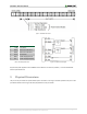
Figure 1. PmodDA2 data stream.
Pin
Signal
Description
1
~SYNC
Chip Select
2
DINA
Data In for Channel A
3
DINB
Data In for Channel B
4
SCLK
Serial Clock
5
GND
Power Supply Ground
6
VCC
Power Supply (3.3V/5V)
Any external power applied to the PmodDA2 must be within 2.7V and 5.5V; however, it is recommended that
Pmod is operated at 3.3V.
3 Physical Dimensions
The pins on the pin header are spaced 100 mil apart. The PCB is 1 inch long on the sides parallel to the pins on the
pin header and 0.8 inches long on the sides perpendicular to the pin header.
Table 1. PmodDA2 pinout table.
Figure 2. PmodDA2 circuit diagram.