Zmod DAC Reference Manual The Digilent Zmod DAC (), is an open-source hardware SYZYGY™ 1) compatible pod containing a dual-channel DAC () and the associated front end. The Zmod DAC () is intended to be used with any SYZYGY™ compatible carrier board having the required capabilities.
Figure 1. Zmod DAC top and bottom views. [] The analog outputs can be connected to a circuit using SMA cables. Driven by the SYZYGY™ carrier, the Zmod DAC () can generate two simultaneous signals (50Ω, ±5V, single-ended, 14-bit, 100MS/s, 40MHz+ bandwidth).
The Zmod DAC () was designed to be a piece in a modular, HW and SW open-source ecosystem. Combined with a SYZYGY™ carrier, other SYZYGY™ compatible pods, Zmod DAC () can be used for a variety of applications: data acquisition systems, closed loop controllers, etc. This document describes the Zmod DAC ()'s circuits, with the intent of providing a better understanding of its electrical functions, operations, and a more detailed description of the hardware’s features and limitations.
2. Arbitrary Waveform Generator 2.1. AWG Reference As shown in Fig. 3, the reference voltage for the AWG is generated by IC42 Initial accuracy: ±0.1% (maximum) Maximum temperature coefficient: 8 ppm/°C Operating temperature range: −40°C to +125°C Output current: +10 mA source/−3 mA sink Low quiescent current: 100 μA (maximum) Low dropout voltage: 250 mV at 2 mA Output noise (0.1 Hz () to 10 Hz ()): <10 μV p-p at 1.
The Analog Devices features are: AD9717 dual, low-power 14-bit TxDAC digital-to-analog converter is used to generate the wave. The main Power dissipation @ 3.3V, 2 mA output: 86 mW @ 125MS/s, sleep mode: <3 mW @ 3.3V Supply voltage: 1.8V to 3.3V SFDR to Nyquist: 84 dBc @ 1 MHz () output, 75 dBc @ 10 MHz () output AD9717 NSD @ 1 MHz () output, 125MS/s, 2 mA: −151 dBc/Hz () Differential current outputs: 1 mA to 4 mA CMOS inputs with single-port operation Output common mode: 0 to 1.
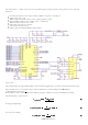
Single-supply 1.8V to 5.5V operation Low on resistance: 2.5 Ω typical 2.3. AWG I/V IC5B in Fig. 5 converts the DAC () output currents to a bipolar voltage. Important AD8058 features: Low cost 325 MHz (), −3 dB bandwidth (G = +1) 1000 V/μs slew rate Gain flatness: 0.1 dB to 28 MHz () Low noise: 7 nV/√Hz Low power: 5.
Figure 5. AWG I/V and Out.
2.4. AWG Out IC8 in Fig. 5 is the output stage of the AWG. features: Low noise: 2.1 nV/√Hz input voltage noise; 2.1 pA/√Hz input current noise Custom compensation Constant bandwidth from G = −1 to G = −10 High speed: 200 MHz () (G = −1), 190 MHz () (G = −10) Low power: 34 mW or 6.7 mA typical for 5 V supply Output disable feature, 1.3 mA Low distortion: −93 dBc second harmonic, fC = 1 MHz (); −108 dBc third harmonic, fC = 1 MHz () DC precision: 1 mV maximum input offset voltage; 0.
2.3. AWG output stage protection Important AD8565 features: Single-supply operation: 4.5 V to 16 V Input capability beyond the rails Rail-to-rail output swing Continuous output current: 35 mA Peak output current: 250 mA Offset voltage: 10 mV Slew rate: 6 V/μs Unity gain stable with large capacitive loads Supply current: 700 μA per amplifier Qualified for automotive applications Low cost The protection circuit in Fig.
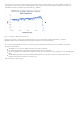
For low frequency range, the spectral characteristic was traced by a network analyzer function, with the ZmodDAC connected to a ZmodADC, as shown in Fig. 7. Since the ZmodADC BW is much wider, the overall system frequency characteristic represents the ZmodDAC characteristic. The BW is flat within 0.1dB up tp 10MHz+. Figure 7. Low frequency AWG spectral characteristics [] However, the figure Fig.
manual) Figure 8. High Frequency AWG spectral characteristics (left), 1dB detail (right) [] The 3dB bandwidth is 40MHz+, the 0.5dB bandwidth is 20MHz+, the ±0.1dB flatness band is 14MHz+. The 3dB bandwidth is close to the theoretical Nyquist limit for a 100MHz sampling system. This has the advantage of very sharp edges (see the rectangular signal in Fig. 9), but also generates alias effects. The ZmodADC generated signals were recorded with a high BW scope in Fig. 9, and the right side of Fig. 10 and Fig.
Figure 9. AWG rectangular signal (large signal) [] Figure 10.
Figure 11. AWG sinusoidal signal (smallsignal); scope set at 20MHz BW limit (left), full BW (right) [] 3. MCU The ATtinny44 MCU works as a I2C memory, storing the SYZYGY™ DNA information and the Calibration Coefficients. The J5 connector is used for programming the MCU and the SYZYGY™ DNA at manufacturing. The DNA and the Factory Calibration Coefficients are stored in the Flash memory of the MCU, which appears to the I2C interface as “read-only”.
Figure 12. The MCU [] Program Memory Type: Flash Program Memory Size (KB): 4 CPU Speed (MIPS/DMIPS): 20 SRAM Bytes: 256 Data EEPROM ()/HEF (bytes): 256 Digital Communication Peripherals: 1-SPI, 1-I2C Capture/Compare/PWM Peripherals: 1 Input Capture, 1 CCP, 4PWM Timers: 1 x 8-bit, 1 x 16-bit Number of Comparators: 1 Temperature Range (C): -40 to 85 Operating Voltage Range (V): 1.8 to 5.5 Pin Count: 14 Low Power: Yes Table 1.
The Zmod DAC () is compliant with SYZYGY™ Specification (https://syzygyfpga.io/specification/). It contains an MCU able to calculate the Geographical Address and provide the DNA information via I2C. The DNA is stored in the MCU FLASH at the address range: 0x8000 - 0x80FF with the following structure: Table 2.
Contents Type Size(Bytes) Value Address Product name string 13 Zmod DAC () 1411 0x8034 Product model / Part number string 13 Zmod DAC () 1411 0x8041 Product version / revision string 1 C 0x804E Serial number string 12 210397000000 0x804F 3.2. Calibration Memory The analog circuitry described in previous chapters includes passive and active electronic components. The datasheet specs show parameters (resistance, capacitance, offsets, bias currents, etc.
Name Size (Bytes) Type Flash Address (Factory Calibration) EEPROM () Address (User Calibration) 4 float32 0x8124 0x7024 Channel 1 Linearity 34 uchar 0x8146 0x7046 Channel 2 Linearity 34 uchar 0x8168 0x7068 Log 22 string 0x817E 0x707E CRC 1 uchar 0x817F 0x707F Heading 1 Channel 2 HG Offset CA Table 4.
Adjustable-output voltage range 0.8 V to 5.0 V (ADP123) Excellent PSRR performance: 60 dB at 100 kHz () Excellent load/line transient response Optimized for small 1.0 μF ceramic capacitors Current limit and thermal overload protection Logic controlled enable Compact packages: 5-lead TSOT and 6-lead 2 mm × 2 mm LFCSP Figure 13. AVCC3V3 [] 4.2. AVCC-2V5 The AVCC-2V5 analog power supply is implemented with the ADP2301 Step-Down regulator in an inverting Buck-Boost configuration.
The user power supplies Fig. 15 use Switching Converter in SEPIC DC-to-DC topology. Main features: 1.4A current limit Minimum input voltage 1.8V Pin-selectable 650 kHz () or 1.3 MHz () PWM frequency Adjustable output voltage up to 20 V Adjustable soft start Undervoltage lockout Figure 15. AVCC8V0 [] The output voltage is: VOU T = VF B ⋅ R80 + R84 = 8.538V (21) R84 Where: VF B = 1.235V typical The supply is enabled after VCC5V0 and AVCC3V3 (see EN_AVCC in Fig. 16) 4.4.
Figure 16. AVCC-8V0 [] The output voltage is: VAV CC8V 0 = −VF B ⋅ R56 R60 = −8.035V (23) Where: VF B = 1.235V typical The supply is enabled after VCC5V0 and AVCC3V3. 5. The SYZYGY™ Connector The SYZYGY™ connector in provides the interface with the carrier board. The used signals are: Power rails VCC5V0 VCC3V3 VADJ - needs to be set by the carier board to 1.
SET_FS_AWG2 DAC () data bus: DIN_AWG_0…13 ADC () SPI bus: CS ()_SC1n SCLK ()_SC SDIO_SC relay control RL_EN_AWG - enables the AWG outputs RESET_AWG Figure 17. SYZYGY™ connector [] 6. The SYZYGY™ compatibility table Table 6. The SYZYGY™ compatibility table [] Parameter Value Maximum 5V supply current 600mA Maximum 3.3V supply current 1mA VIO supply voltage 1.
Parameter Value Maximum VIO supply current 10mA Total number of I/O 21 Number of differential I/O pairs 0 Width Single Written by Mircea Dabacan, PhD, Technical University of Cluj-Napoca Romania 1) The “SYZYGY™ ” mark is owned by Opal Kelly.


