
Datasheet

ZXGD3006E6
Document Number DS35229 Rev. 4 - 2
2 of 8
www.diodes.com
June 2013
© Diodes Incorporated
A
Product Line o
f
Diodes Incorporated
ZXGD3006E6
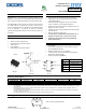
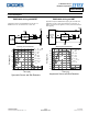
Typical Application Circuit
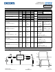
Maximum Ratings (@T
A
= +25°C, unless otherwise specified.)
Characteristic Symbol Value Unit
Supply voltage, with respect to V
EE
V
CC
40 V
Input voltage, with respect to V
EE
V
IN
40 V
Output difference voltage (Source – Sink)
V
(source-sink)
±7.5 V
Peak output current
I
PK
±10 A
Input current
I
IN
±100 mA
Thermal Characteristics (@T
A
= +25°C, unless otherwise specified.)
Characteristic Symbol Value Unit
Power Dissipation (Notes 6 & 7)
Linear derating factor
P
D
1.1
8.8
W
mW/°C
Thermal Resistance, Junction to Ambient (Notes 6 & 7)
R
JA
113
°C/W
Thermal Resistance, Junction to Lead (Note 8)
R
JL
105
Operating and Storage Temperature Range
T
J,
T
STG
-55 to +150 °C
ESD Ratings (Note 9)
Characteristic Symbol Value Unit JEDEC Class
Electrostatic Discharge - Human Body Model ESD HBM 1,500 V 1C
Electrostatic Discharge – Charged Device Model ESD CDM 1,000 V IV
Notes: 6. For a device mounted on 25mm x 25mm 1oz copper that is on a single-sided 1.6mm FR4 PCB; device is measured under still air conditions whilst
operating in a steady-state. The heatsink is split in half with the pin 1 (V
CC
) and pin 3 (V
EE
) connected separately to each half.
7. For device with two active die running at equal power.
8. Thermal resistance from junction to solder-point at the end of each lead on pin 1 (V
CC
) and pin 3 (V
EE
).
9. Refer to JEDEC specification JESD22-A114 and JESD22-C101.
IN
V
CC
+ supply
ZXGD3006
V
S
V
CC
SOURCE
SINK
R
SOURCE
R
SINK
Controller
V
EE
IGBT
(or SiC MOSFET)
V
EE
- supply