PSG1302028CE CD Stereo System Model No. SA-AKX36PH SA-AKX36PN Product Color: (K)...Black Type Please refer to the original service manual for: CD Mechanism Unit , Order No. PSG1102001CE O Speaker system SB-AKX36PN-K, Order No. PSG1302023CE O TABLE OF CONTENTS PAGE 1 Safety Precautions----------------------------------------------- 3 1.1. General Guidelines---------------------------------------- 3 1.2. Before Use (For PH only)-------------------------------- 4 1.3.
8 Service Mode ----------------------------------------------------- 19 8.1. Cold-Start--------------------------------------------------- 19 8.2. Doctor Mode Table--------------------------------------- 20 8.3. Reliability Test Mode (CD Mechanism Unit) ------- 23 8.4. Self-Diagnostic Mode ----------------------------------- 24 8.5. Self-Diagnostic Error Code Table -------------------- 24 8.6.
1 Safety Precautions 1.1. General Guidelines 1. IMPORTANT SAFETY NOTICE There are special components used in this equipment which are important for safety. These parts are marked by in the Schematic Diagrams, Circuit Board Layout, Exploded Views and Replacement Parts List. It is essential that these critical parts should be replaced with manufacturer’s specified parts to prevent X-RADIATION, shock, fire, or other hazards. Do not modify the original design without permission of manufacturer. 2.
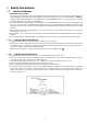
1.2. Before Use (For PH only) Be sure to disconnect the mains cord before adjusting the voltage selector as shown in Figure 1-2 Use a minus(-) screwdriver to set the voltage selector (on the rear panel) to the voltage setting for the area in which the unit will be used. Note that this unit will be seriously damaged if this setting is not made correctly. (There is no voltage selector for some countries, the correct voltage is already set.) Figure 1-2 1.3.
1.5. Power Supply using SMPS This model uses SMPS Module to Power up the unit. Below is the part number of the SMPS Model. N0AB3GL00001 (PN) N0AD3GL00001 (PH) 1.5.1. For SA-AKX36PN Figure 1-3 1.5.2.
1.6. Safety Parts Information Safety Parts List: There are special components used in this equipment which are important for safety. These parts are marked by in the Schematic Diagrams, Exploded View & Replacement Parts List. It is essential that these critical parts should be replaced with manufacturer’s specified parts to prevent shock, fire or other hazards. Do not modify the original design without permission of manufacturer. Safety Ref No. Part No.
2 Warning 2.1. Prevention of Electrostatic Discharge (ESD) to Electrostatically Sensitive (ES) Devices Some semiconductor (solid state) devices can be damaged easily by static electricity. Such components commonly are called Electrostatically Sensitive (ES) Devices. The following techniques should be used to help reduce the incidence of component damage caused by electrostatic discharge (ESD). 1.
2.2. Precaution of Laser Diode Caution: This product utilizes a laser diode with the unit turned “on”, invisible laser radiation is emitted from the pickup lens. Wavelength: 790 nm (CD) Maximum output radiation power from pickup: 100 µW/VDE Laser radiation from the pickup unit is safety level, but be sure the followings: 1. Do not disassemble the pickup unit, since radiation from exposed laser diode is dangerous. 2. Do not adjust the variable resistor on the pickup unit. It was already adjusted. 3.
2.3. Service caution based on Legal restrictions 2.3.1. General description about Lead Free Solder (PbF) The lead free solder has been used in the mounting process of all electrical components on the printed circuit boards used for this equipment in considering the globally environmental conservation. The normal solder is the alloy of tin (Sn) and lead (Pb).
2.4. Handling Precautions for Traverse Unit The laser diode in the optical pickup unit may break down due to static electricity of clothes or human body. Special care must be taken avoid caution to electrostatic breakdown when servicing and handling the laser diode in the traverse unit. 2.4.1. Cautions to Be Taken in Handling the Optical Pickup Unit The laser diode in the optical pickup unit may be damaged due to electrostatic discharge generating from clothes or human body.
2.5. Grounding for electrostatic breakdown prevention • As for parts that use optical pick-up (laser diode), the optical pick-up is destroyed by the static electricity of the working environment. Repair in the working environment that is grounded. 2.5.1. Worktable grounding • Put a conductive material (sheet) or iron sheet on the area where the optical pickup is placed and ground the sheet. 2.5.2.
3 Service Navigation 3.1. Service Information This service manual contains technical information which will allow service personnel’s to understand and service this model. Please place orders using the parts list and not the drawing reference numbers. If the circuit is changed or modified, this information will be followed by supplement service manual to be filed with original service manual. • CD Mechanism Unit: 1) This model uses CD Mechanism Unit.
3.2.
4 Specifications Q Amplifier section RMS output power stereo mode Front Ch (both ch driven) Total RMS stereo mode power Q Tuner, terminals section Preset memory Frequency modulation (FM) Frequency range Antenna terminals Amplitude modulation (AM) Frequency range Music port (front) Sensitivity Terminal Aux Input Q Disc section Discs played (8 cm or 12 cm) Pick up Wavelength Audio output Number of channels FL = Front left channel FR = Front right channel *MPEG-1 Layer 3 Q General Power supply Power consum
5 General/Introduction 5.1.
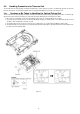
6 Location of Controls and Components 6.1.
6.2.
7 Installation Instructions 7.1.
8 Service Mode 8.1. Cold-Start Here is the procedure to carry out cold-start or initialize to shipping mode. 1. Unplug AC power cord 2. Press & hold [POWER] button 3. Plug AC power cord while [POWER] button being pressed FL Display will show “_ _ _ _ _ _ _ _” 4.
8.2. Doctor Mode Table 8.2.1. Doctor Mode Table 1 Item Mode Name Doctor Mode Key Operation FL Display Description To enter into Doctor Mode Front Key In CD Mode: 1. Press [ ] button on main unit follow by [4] and [7] on remote control. 2. To exit, press [DELETE] button on remote control or, press [POWER, /I] button on Main Unit EEPROM checksum check Displaying of 1. Year Develop. 2. Model Type. 3. ROM Type. 4. Firmware Version. In CD mode: 1.
8.2.2. Doctor Mode Table 2 Key Operation Item Mode Name Volume Setting Check FL Display Description Front Key To check the volume setting of the main unit. In Doctor Mode: 1. Press [7], [8], [9] button on the remote control. Press [7]: VOL50 Press [8]: VOL35 Press [9]: VOL0 Volume FL Display Check To check the FL segment display. All segments will light up while all LED blink at 0.5s intervals. In Doctor mode: 1. Press [1] button on the remote control. 2.
8.2.3. Doctor Mode Table 3 Key Operation Item Mode Name CD Self- Adjustment Test FL Display Description Front Key To display result of self-adjustment for CD. In Doctor Mode: 1. Press [10] [1] [4] button on the remote control.
8.3. Reliability Test Mode (CD Mechanism Unit) Below is the process flow chart of the aging test for the CD Mechanism Unit . OPEN Operation First Track Access OPEN wait for 1 s CLOSE Operation First Track Play 5 s Count up Last Track Access Last Track Play 5 s CLOSE wait for 4 s Fig. 1. Reliability Test (Loading) Count up Fig. 2.
8.4. Self-Diagnostic Mode Item Mode Name Self Diagnostic Mode FL Display Description Key Operation Front Key To enter into self diagnostic checking Step 1: Select CD mode (Ensure no disc is inserted). Step 2: Press & hold [ ] button follow by [ / ] on main unit for 2 seconds. Error code information System will perform a check on any unusual/error code from the memory Example: Step 1: In self diagnostic mode, Press [ ] on main unit. To exit, press [^/I] on main unit or remote control.
8.5.2. CD Mechanism Error Code Table (CD Mechanism Unit) Error Code Diagnostic Contents Description of error Automatic FL Display Remarks CD H15 CD Open Abnormal During operation POS_SW_R On fail to be detected with 4 sec. Error No. shall be clear by force or during cold start. Press [ ] on main unit for next error. CD H16 CD Closing Abnormal During operation POS_SW_CEN On fail to be detected with 4 sec. Error No. shall be clear by force or during cold start.
9 Troubleshooting Guide "Contents for this section is not available at time of issue" 26
10 Disassembly and Assembly Instructions • Illustration is based on SA-AKX36PH-K. Caution Note: • This section describes the disassembly and/or assembly procedures for all major printed circuit boards & main components for the unit. (You may refer to the section of “Main components and P.C.B Locations” as described in the service manual) • Before carrying out the disassembly process, please ensure all the safety precautions & procedures are followed.
10.2. Disassembly Flow Chart 10.4.Top Cabinet 10.5. Front panel Unit 10.16. Fan Unit 10.10. Rear Panel 10.6. Panel P.C.B., LED P.C.B. and Mic P.C.B. 10.11. Main P.C.B. 10.7. Remote Sensor P.C.B. 10.12.Digital Amplifier IC (IC6000) 10.8. USB P.C.B. 10.13.SMPS Module and Voltage Selector P.C.B. 10.9. CD Lid 10.14. CD Mechanism Unit 10.15. CD Interface P.C.B.
10.3. Main Components and P.C.B.
10.4. Disassembly of Top Cabinet Step 4 Slightly lift up both sides of Top Cabinet in an outward direction as shown. Step 5 Remove the Top Cabinet. Step 1 Remove 2 screws on each side. Step 2 Remove 5 screws. Step 3 Slightly pull both side of Top Cabinet outwards as arrow shown. Caution: During assembling, ensure that the Top Cabinet catches are properly inserted into Front Panel Unit.
10.5. Disassembly of Front Panel Unit Step 3 Release tab at the left side of Front Panel Unit. • Refer to “Disassembly of Top Cabinet”. Step 1 Detach 5P Cable at the connector (CN2002) on Main P.C.B.. Step 2 Detach 30P FFC at the connector (CN2000) on Main P.C.B..
Step 4 Release tabs at bottom. Step 6 Remove the Front Panel Unit as arrow shown. 10.6. Disassembly of Panel P.C.B., LED P.C.B. and Mic P.C.B. • Refer to “Disassembly of Top Cabinet”. • Refer to “Disassembly of Front Panel Unit”. Step 5 Release tab at the right side of Front Panel Unit. Step 1 Remove the Volume Knob. Step 2 Remove the Control Knob.
Step 3 Remove 7 screws. Step 5 Lift up the Panel P.C.B. and LED P.C.B. from Front Panel Unit. Step 4 Release catches by following the sequences (1-8). Caution: During assembling, ensure that LED P.C.B. is properly insert to Front Panel Unit.
Caution: During assembling, ensure that Mic P.C.B. is seated properly through the located & fully catched. Caution: During assembling, ensure that Panel P.C.B. is seated properly through the located & fully catched. 10.7. Disassembly of Remote Sensor P.C.B. • Refer to “Disassembly of Top Cabinet”. • Refer to “Disassembly of Front Panel Unit”. • Refer to “Disassembly of Panel P.C.B., LED P.C.B. and Mic P.C.B.”. Step 1 Remove the Remote Sensor P.C.B.. Caution: During assembling, ensure that Remote Sensor P.
10.8. Disassembly of USB P.C.B. 10.9. Disassembly of CD Lid • Refer to “Disassembly of Top Cabinet”. • Refer to “Disassembly of Front Panel Unit”. • Refer to “Disassembly of Top Cabinet”. • Refer to “Disassembly of Front Panel Unit”. Step 1 Remove 1 screw. Step 2 Release 1 catch. Step 3 Remove the USB P.C.B.. Step 1 Remove the spring as arrow shown in order of sequence (1) to (3). Caution: During assembling, ensure that the spring is assembly at correct position.
10.10. Disassembly of Rear Panel Step 5 Lift up Inner Chassis Unit to release the catch between the Inner Chassis Unit and the Rear Panel. • Refer to “Disassembly of Top Cabinet”. Step 1 Remove 10 screws. Step 6 Release 2 tabs. Step 7 Remove Rear Panel. Step 2 Detach Voltage Selector P.C.B. from Rear Panel as arrow shown. Step 3 Release 1 catch at the Fan Unit . Step 4 Remove the Fan Unit .
10.11. Disassembly of Main P.C.B. Step 8 Remove the Main P.C.B.. Caution: During assembling, ensure that Main P.C.B. is seated properly through the located & fully guided. • Refer to “Disassembly of Top Cabinet”. • Refer to “Disassembly of Rear Panel”. Step 1 Detach 5P Cable at the connector (CN2002) on Main P.C.B.. Step 2 Detach 30P FFC at the connector (CN2000) on Main P.C.B.. Step 3 Detach 13P Cable at the connector (CON2) on SMPS Module. Step 4 Detach 10P FFC at the connector (CN8251) on Main P.C.B..
10.12. Disassembly of Digital Amplifier IC (IC6000) Step 4 Desolder the pins of the Digital Amplifier IC (IC6000). Step 5 Remove the Digital Amplifier IC (IC6000). • Refer to “Disassembly of Main P.C.B.”. 10.12.1. Disassembly of Digital Amplifier IC (IC6000) Caution: Handle the Main P.C.B. with caution due to it’s high temperature after prolonged use. Touching it may lead to injuries. Step 1 Place the Main P.C.B. on an insulated material. Step 2 Remove 2 screws. 10.12.2.
10.13. Disassembly of SMPS Module and Voltage Selector P.C.B. Step 3 Fix Heatsink spacers onto Main Heatsink.. Caotion: Ensure that the Heatsink Spacers are properly located and seated flatly onto Main Heatsink. Step 4 Apply grease to the Main Heatsink as indicate in the diagram. Caution: Ensure Grease thickness is about 0.2mm. • Refer to “Disassembly of Top Cabinet.”. • Refer to “Disassembly of Rear Panel”. Step 1 Detach 13P Cable at a connector (CON2) on the SMPS Module. Step 2 Remove 2 screws.
10.14. Disassembly of CD Mechanism Unit Step 2 Detach Voltage Selector P.C.B. from the Rear Panel. Step 3 Detach 10P FFC at a connector (CN8251) on Main P.C.B.. Step 4 Detach 24P FFC at a connector (FP8201) on Main P.C.B.. Step 5 Detach 2P Wire at a connector (CN1001) on Main P.C.B.. Step 6 Remove 1 screw. • Refer to “Disassembly of Top Cabinet”. • Refer to “Disassembly of Front Panel Unit”. Step 1 Remove 8 screws. Step 7 Remove 1 screw.
Step 10 Remove 2 screws. Step 11 Remove the CD Mechanism Unit. Step 8 Release 2 catches. Step 9 Lift up and remove the Inner Chassis Unit. 10.15. Disassembly of CD Interface P.C.B. • Refer to “Disassembly of Top Cabinet”. • Refer to “Disassembly of Front Panel Unit”. • Refer to “Disassembly of CD Mechanism Unit”. Caution: During assembling, ensure that Inner Chassis Unit is catched onto Rear Panel properly. Step 1 Remove 3 screws. Step 2 Desolder pins of the motor (M7301).
10.16. Disassembly of Fan Unit • Refer to “Disassembly of Top Cabinet”. Step 1 Remove 1 screw. Step 2 Detach 2P Wire at a connector (CN1001) on the Main P.C.B.. Step 3 Release 1 catch. Step 4 Remove the Fan Unit. Caution: During assembling, ensure that Fan Unit is catched onto Rear Panel properly.
11 Service Position 11.2. Checking of Main P.C.B. (Side B) Note: For description of the disassembly procedures, see the Section 10. 11.1. Checking of Panel P.C.B., LED P.C.B. and Mic P.C.B. Step 1 Remove Top Cabinet. Step 2 Remove Rear Panel. Step 3 Remove Main P.C.B.. Step 4 Remove 2 screws. Step 1 Remove Top Cabinet. Step 2 Remove Front Panel Unit. Step 3 Remove the Panel P.C.B., the LED P.C.B. and Mic P.C.B.. Step 4 Positioned the Panel P.C.B., the LED P.C.B. and Mic P.C.B.
11.3. Checking of Main P.C.B. (Side A) Step 6 Attach 13P Cable at a connector (CON2) on the SMPS Module. Step 7 Attach 30P FFC at a connector (CN2000) on the Main P.C.B.. Step 8 Attach 10P FFC at a connector (CN8251) on the Main P.C.B.. Step 9 Attach 24P FFC at a connector (FP8201) on the Main P.C.B.. Step 10 Attach 2P FFC at a connector (CN1001) on the Main P.C.B.. Step 11 Side B Main P.C.B. can be checked at diagram shown. Step 1 Remove Top Cabinet. Step 2 Remove Front Panel Unit.
12 Block Diagram 12.1. Servo & System Control : CD AUDIO INPUT SIGNAL LINE : USB SIGNAL LINE : AUDIO OUTPUT SIGNAL LINE MAIN P.C.B. IC8001 MN6627992AB SERVO PROCESSOR USB P.C.B.
: CD AUDIO INPUT SIGNAL LINE : USB SIGNAL LINE : AUDIO OUTPUT SIGNAL LINE MAIN P.C.B. IC2006 RFKWMAKX36LM PANEL P.C.B. MICROPROCESSOR QR6001, QR6003,QR6004 LED DIMMER 78 LED RED 82 LED GREEN 83 LED DIMMER CN2000 CN6001 3 CN2000 CN6001 GREEN LED CN2000 CN6001 27 28 +5V LED DIMMER LED CA 28 RED LED MEMORY LED P.C.B.
12.2.
12.3. Audio : CD AUDIO INPUT SIGNAL LINE : AUX/TUNER/MUSIC PORT AUDIO INPUT SIGNAL LINE : AM SIGNAL LINE : AUDIO OUTPUT SIGNAL LINE : FM SIGNAL LINE MAIN P.C.B. IC6100 C0JBAR000367 AUDIO SELECTOR ANA SEL2 ANA SEL2 ANA SEL1 ANA SEL1 9 A(LSB) 10 B(MSB) QR6100 FROM/TO SERVO & SYSTEM CONTROL MPORT SW SWITCH MPORT SW MUSIC PORT P.C.B.
12.4. Power Supply MAIN P.C.B. SMPS MODULE PW +32.5V PW SYS3R3V - CN1000* - 6 +32.5V +3.
MAIN P.C.B. PW 6V +6V IC1000 C0DBGYY03909 +3.3V VOLTAGE REGULATOR 2 PW 6V PW +6V VOUT 2 3 VIN PW 3V3,PW 3R3V DIG,PW 3R3V DAC,PW 3R3V CD PW 3V3 +3.3V D1001 D1002 DC DET PWR DC DET PWR QR1000 DC DETECT Q1000 PW 16V +12V VOLTAGE REGULATOR PW 12V PW 12V +12V D1005 5 PW +16V PANEL P.C.B. VP DET CN2000 CN6001 25 VP DET 6 T6000 SWITCHING TRANSFORMER Q6001 -VP -VP +16V CN2000 CN6001 23 1 PW +5V CN2000 CN6001 +5V CN2000 CN6001 1 PW SYS3R3V 8 CD3.3V 2 3 SYS3.
13 Wiring Connection Diagram TO SMPS MODULE P.C.B. JK6000 CN6001 21 1 1 CN1000* 2 13 TO SPEAKERS 3 1 4 CN6002 4 29 30 JK6002 A 3 AUX IN 1 MAIN P.C.B. VR6100 (SIDE B) 2 B CN2000 1 30 2 4 1 2 3 PANEL P.C.B.
14 Schematic Diagram 14.1. Schematic Diagram Notes • This schematic diagram may be modified at any time with the development of new technology. Notes: S6000: S6001: S6002: S6003: S6004: S6006: S6012: S6100: S6101: S6103: S6104: S6105: S6107: S6200: S6201: S6202: S6203: S6204: S6206: S6207: S6208: S7201: VR6100: VR6200: Playlist 2 switch. Playlist 3 switch. Playlist 4 switch. Playlist 1 switch. Playlist 5 switch. Playlist 6 switch. Stop ( ) /Tune Mode switch. CD switch. Radio/EXT-IN switch.
14.2. MAIN (CD Servo/Micon/Damp) Circuit 1 A 2 3 4 5 6 7 8 9 10 11 12 13 14 SCHEMATIC DIAGRAM - 1 A MAIN (CD SERVO) CIRCUIT : +B SIGNAL LINE : AUDIO OUTPUT SIGNAL LINE : CD AUDIO INPUT SIGNAL LINE : USB SIGNAL LINE 41 MSDWP 0 CMD_EMMC R8026 0 C8037 0.1 C8038 0.1 1 0.1 C8060 C8031 D3 D4 0.
15 16 17 18 19 20 21 22 23 24 25 26 27 28 SCHEMATIC DIAGRAM - 2 A MAIN (CD SERVO) CIRCUIT : +B SIGNAL LINE : AUDIO OUTPUT SIGNAL LINE : CD AUDIO INPUT SIGNAL LINE : USB SIGNAL LINE P1 P1 FP8201 F- 24 F- F+ 23 F+ T+ 22 T+ T- 21 T- C R8201 0 D R8202 0 A R8203 0 B R8204 0 F R8205 0 20 C 19 D 18 CD/DVD SW 17 RF 16 A 15 B 14 F TO OPTICAL PICKUP UNIT (CD MECHANISM UNIT BRS11C) 13 PD_GND MI PW_5V LB8204 J0JBC0000134 LB8202 J0JHC0000045 12 VREF 11 VCC(5V) E LDM
29 30 31 32 33 34 35 36 37 38 39 40 41 42 SCHEMATIC DIAGRAM - 3 A A MAIN (CD SERVO) CIRCUIT : +B SIGNAL LINE : AUDIO OUTPUT SIGNAL LINE : CD AUDIO INPUT SIGNAL LINE : USB SIGNAL LINE C8509 0.1 LB8501 J0JHC0000045 C8513 4.7 C8508 0.1 B IO3SF R8017 0 7 HOLD# SO 2 6 SCLK IO0SF R8015 0 C8401 10 0 80 VSS IO2SF VSS 4 IC8401 C3FBMY000309 16M FLASH MEMORY C8510 0.
2 1 A 3 4 5 6 7 8 9 10 11 12 13 14 SCHEMATIC DIAGRAM - 4 A MAIN (MICON) CIRCUIT : +B SIGNAL LINE : CD AUDIO INPUT SIGNAL LINE : AUDIO OUTPUT SIGNAL LINE : FM SIGNAL LINE : -B SIGNAL LINE : AUX/TUNER/MUSIC PORT AUDIO INPUT SIGNAL LINE : AM SIGNAL LINE : USB SIGNAL LINE P1 CD: MAIN (CD SERVO): SCHEMATIC DIAGRAM - 1 ~ 3 DA: MAIN (DAMP): SCHEMATIC DIAGRAM - 8 D2001 DA2J10100L B 560K R2084 REC_LED JOG_ROTA JOG_ROTB AM_BP CD CD CD CD R2310 R2312 R2313 0 0 0 CD_MLD CD_MDATA CD_STAT
15 16 17 18 19 20 21 22 23 24 25 26 27 28 SCHEMATIC DIAGRAM - 5 A MAIN (MICON) CIRCUIT : +B SIGNAL LINE : CD AUDIO INPUT SIGNAL LINE : AUDIO OUTPUT SIGNAL LINE : FM SIGNAL LINE : -B SIGNAL LINE : AUX/TUNER/MUSIC PORT AUDIO INPUT SIGNAL LINE : AM SIGNAL LINE : USB SIGNAL LINE A B R8041 0 PW_3V3 D6501 DA2J10100L R6514 470 C6505 0.047 2 PWM_HPP_L NC 55 3 PWM_HPM_R NC 54 4 PWM_HPP_R NC 53 5 AVSS C6504 R6503 0 C6501 0.
I SCHEMATIC DIAGRAM - 6 A MAIN (MICON) CIRCUIT : +B SIGNAL LINE : CD AUDIO INPUT SIGNAL LINE : AUDIO OUTPUT SIGNAL LINE : FM SIGNAL LINE : -B SIGNAL LINE : AUX/TUNER/MUSIC PORT AUDIO INPUT SIGNAL LINE : AM SIGNAL LINE : USB SIGNAL LINE TO MAIN (MICON) CIRCUIT (1/4) P1 OC IC2030 C0DBZYY00311 J HIGH SIDE SWITCH EN 4 /OC EN 3 GND 2 C2017 0.
SCHEMATIC DIAGRAM - 7 : +B SIGNAL LINE : CD AUDIO INPUT SIGNAL LINE : AUDIO OUTPUT SIGNAL LINE : FM SIGNAL LINE : -B SIGNAL LINE : AUX/TUNER/MUSIC PORT AUDIO INPUT SIGNAL LINE : AM SIGNAL LINE : USB SIGNAL LINE P1 A MAIN (MICON) CIRCUIT I TO MAIN (MICON) CIRCUIT (2/4) J PCONT POWER P1 CN1000* ECO_CTR 13 ECO_CTR 12 POWER C1005 SYNC TEMP_DET 0.
1 A 2 3 4 5 6 7 8 9 10 11 12 13 14 SCHEMATIC DIAGRAM - 8 A A MAIN (DAMP) CIRCUIT : +B SIGNAL LINE : AUDIO OUTPUT SIGNAL LINE B B HEATSINK* G1 C R6050 10 R6007 10 C6005 10 C6018 0.1 C6019 0.1 R6046 22K G2 IC6000 C1AB00003986 POWER AMPLIFIER 1 GVDD_AB BST_A 44 2 VDD BST_B 43 3 OC_ADJ VALID 4 /RESET MI PWM_P_1 5 INPUT_A OUT_A 40 MI PWM_M_1 6 INPUT_B OUT_A 39 MI C6023 0.
14.3.
15 16 17 18 19 20 21 22 23 24 25 26 27 28 SCHEMATIC DIAGRAM - 10 A B PANEL CIRCUIT : +B SIGNAL LINE : -B SIGNAL LINE : MUSIC PORT AUDIO INPUT SIGNAL LINE P1 B CN6001 30 1 NC 2 NC GREEN_LED 3 LED_GREEN RED_LED 4 LED_RED 5 NC 6 VP_DET -VP FL_GND 7 DGND PW_+15V 8 +15V 9 MPORT_R MPORT_R MPORT_GND 11 MPORT_L 12 MPORT_SW MPORT_SW JOG_ROTA 13 JOG_ROTA 14 JOG_ROTB JOG_ROTB JOG_VOLA E TO MEMORY LED CIRCUIT (ZJ6700*) IN SCHEMATIC DIAGRAM - 11 15 JOG_VOLA 16 JOG_VOLB JOG_VOLB LE
14.4.
15 Printed Circuit Board 15.1. Main P.C.B.
Q1000 10 15 20 CK2208 CK2202 R2336 C1002 R1000 R2120 C8059 R2341 C8058 R2333 C8032 R9003 C2064 10 11 12 3 13 14 R2000 15 16 R2313 R2312 1 17 18 R8029 LB8002 R8032 9 X2002 X2001 19 20 21 22 23 105 108 1 3 5 7 9 21 30 C8256 R8263 3 B 4 Q2500 R1024 C1012 R1018 B E D1004 C1010 B R1013 E C2018 Q1001 B R1014 C R1015 C C R2504 E QR2500 E C B Q1004 Q1002 Q1005 R2503 CN2002 5 C C2017 4 3 2 1 2 3 E C1014 8 R1012 4 IC1001 1 4 R1011 R1010 B R1
15.2. Panel, USB, Music Port & Memory LED P.C.B. B C PANEL P.C.B. (REP4884CA) USB P.C.B.
15.3. Remote Sensor & CD Interface P.C.B. F G REMOTE SENSOR P.C.B. (REP4884CE) CD INTERFACE P.C.B. (REP4945A) H M7302* PbF 3646AE 2 3 4 CN6500 (SPINDLE MOTOR) C6501 C6500 1 1 IR6500 G 3 2 1 2 S7201 (RESET) SENSOR CN7002 9 7 5 2 4 1 3 10 8 6 4 3 2 1 F CN7001 M7301* 2 TO LOADING P.C.B. (CD MECHANISM UNIT BRS11C) (TRAVERSE MOTOR) 4 1 5 2 3 1 PbF 3556A E D C B A NOTE: " * " REF IS FOR INDICATION ONLY 1 2 3 SA-AKX36PH/PN REMOTE SENSOR / CD INTERFACE P.C.B.
16 Appendix Information of Schematic Diagram 16.1. Voltage & Waveform Chart Note: • Indication Voltage Values are in standard values for the unit measured by the DC electronic circuit tester (high-impedance) with the chassis taken as standard. Therefore, there may exist some errors in voltage values, depending on the internal impedance of the DC circuit tester.
16.1.2. Main P.C.B. (2/5) IC2007 REF NO. MODE CD PLAY STANDBY 1 0 0 2 0 0 3 0 0 4 0 0 5 0 0 REF NO. MODE CD PLAY STANDBY 1 5.2 5.2 2 0 0 3 3.3 3.3 4 3.3 3.3 5 5.2 5.2 REF NO. MODE CD PLAY STANDBY 1 2 12.1 12.2 12.1 12.2 3 1.2 1.2 4 2.5 2.5 5 1.6 1.6 6 1.6 1.6 7 2.7 2.7 22 23 24 12.1 27.9 27.0 12.1 27.9 27.0 25 0 0 26 0 0 27 28 29 30 31 32 16.4 16.4 32.0 32.0 32.0 16.4 16.4 16.4 32.0 32.0 32.0 16.4 6 0 0 7 0 0 8 3.3 3.3 IC2030 IC6000 8 3.2 3.2 9 0 0 10 0 0 11 0 0 12 0 0 13 7.
16.1.3. Main P.C.B. (3/5) IC7704 REF NO. MODE CD PLAY STANDBY 21 0 0 22 1.7 1.7 23 1.8 1.8 24 1.6 1.6 25 3.3 3.3 26 0 0 27 1.6 1.6 28 1.6 1.6 29 1.7 1.7 30 1.7 1.7 REF NO. MODE CD PLAY STANDBY 41 0 0 42 1.3 1.3 43 1.3 1.3 44 3.3 3.3 45 1.3 1.3 46 1.3 1.3 47 0 0 48 1.3 1.3 49 1.3 1.3 50 0 0 REF NO. MODE CD PLAY STANDBY 1 3.2 3.2 2 1.3 1.3 3 1.1 1.1 4 1.2 1.2 5 1.2 1.2 6 1.3 1.3 7 3.2 3.2 8 1.2 1.2 9 0 0 10 3.2 3.2 REF NO.
16.1.4. Main P.C.B. (4/5) IC8251 REF NO. MODE CD PLAY STANDBY 1 1.7 1.7 2 0 0 3 0 0 4 1.6 1.6 5 0 0 6 3.0 3.1 7 3.0 3.0 8 5.8 5.8 9 0 0 10 0 0 REF NO. MODE CD PLAY STANDBY 21 1.5 1.0 22 0 0 23 1.6 1.7 24 0 0 25 0 0 26 1.7 1.7 27 1.7 1.7 28 3.3 3.3 29 0 0 30 0 0 REF NO. MODE CD PLAY STANDBY 1 2.1 2.4 2 2.6 2.6 3 3.3 3.3 4 0 0 5 3.0 3.2 6 0.6 0.5 7 3.3 3.3 8 3.3 3.3 REF NO. MODE CD PLAY STANDBY 1 0 0 2 1.0 1.0 3 1.2 1.2 4 1.2 1.2 5 1.2 1.2 6 0 0 7 0 0 8 3.3 3.
16.1.5. Main P.C.B. (5/5) IC8501 REF NO. MODE CD PLAY STANDBY 141 0 0 REF NO. MODE CD PLAY STANDBY Q1000 Q1001 E C B 12.4 12.4 12.0 12.4 12.4 12.0 E C B 16.0 16.0 12.0 16.0 16.0 12.0 REF NO. MODE CD PLAY STANDBY E 3.3 3.3 REF NO. MODE CD PLAY STANDBY REF NO. MODE CD PLAY STANDBY 142 3.3 3.3 143 0 0 144 3.3 3.3 145 0 0 Q1005 C 16.0 16.0 146 0 0 147 0 0 148 0 0 149 0 0 E 0 0 C 7.0 7.0 E 5.0 5.0 Q6007 Q6300 E C B 15.7 15.3 16.1 16.2 15.8 16.2 E C B 16.2 15.8 16.2 16.0 16.0 16.0 E 3.
16.1.7. Waveform Table WF No. IC2006-12 (PLAY) WF No. IC2006-13 (PLAY) WF No. IC2006-15 (PLAY) WF No. IC2006-16 (PLAY) 4Vp-p(50nsec/div) 3.2Vp-p(50nsec/div) 1.8Vp-p(10usec/div) 2.8Vp-p(10usec/div) WF No. IC6000-5,6,14,15 (PLAY) WF No. IC6000-27,28,32,35,39,40 (PLAY) WF No. IC6500-24 (PLAY) WF No. IC6500-25 (PLAY) 2.4Vp-p(1usec/div) 32Vp-p(1usec/div) 3.4Vp-p(500nsec/div) 3.2Vp-p(10usec/div) WF No. IC6500-38,39,40,41 (PLAY) WF No. IC8001-89,90 (PLAY) WF No. IC8001-117 (PLAY) 2.
17 Exploded View and Replacement Parts List 17.1. Exploded View and Mechanical replacement Part List 17.1.1. Cabinet Parts Location c *ZJ6700 (MEMORY LED P.C.B.) FL6000 H 22 19 19 19 7 c 24 CN6003 17 G 19 (PANEL P.C.B.) 43 20 CN6002 22 19 CN6500 IR6500 VR6200 (REMOTE SENSOR P.C.B.) 22 F T6000 19 30 20 19 44 31 CN6001 VR6100 *ZJ6000 6 3 E k a 19 22 20 29 *ZJ6400 (USB P.C.B.) b 22 34 19 k 36 (MUSIC PORT P.C.B.
H e f a G 16 21 2 JK52 JK6002 JK51 CN1001 23 FP9003 b 23 JK6000 i j 4 (FOR PH ONLY) 14 CN8251 CN2002 F 22 *D-AMP HEATSINK UNIT 21 22 22 22 22 14 (BRS11C) CN2001 (MAIN P.C.B.) CN2000 FP8201 h 18 d 21 18 *CN1000 d g h 5 E 22 (FOR PH ONLY) 22 21 i 22 15 22 22 f 301 8 21 (SMPS MODULE) D 21 25 1 21 e C 21 CN7002 (CD INTERFACE P.C.B.
17.1.2.
17.1.3. Mechanical Replacement Part List Safety Safety Ref. No. Part No.
Safety Ref. No. 42 Part No.
17.2. Electrical Replacement Part List Safety Safety Ref. No. Part No. Part Name & Qty Description PRINTED CIRCUIT BOARDS Remarks PCB1 REP4902G MAIN P.C.B. 1 PCB2 REP4902F MAIN P.C.B. 1 PCB3 PCB4 PCB5 REP4884CA REP4884CB REP4884CA 1 1 1 PCB6 REP4884CA 1 (RTL) PCB7 REP4884CE 1 (RTL) PCB8 REP4945A 1 (RTL) PCB9 N0AB3GL00001 PANEL P.C.B. USB P.C.B. MUSIC PORT P.C.B. MEMORY LED P.C.B. REMOTE SENSOR P.C.B. CD INTERFACE P.C.B.
Safety Ref. No. D1000 D1001 D1002 D1004 D1005 D2001 D2002 D6005 D6006 D6007 D6008 D6009 D6012 D6102 D6103 D6104 D6105 D6400 D6501 D6700 D8250 DZ1000 DZ2001 Part No.
Safety Ref. No. W1001 W1002 W1003 W1004 W1005 W1006 W1007 W1008 W1009 W1010 W1011 W1012 W1014 W1015 W1016 W1017 W1018 W1019 W1020 W1021 W1022 W1023 W1024 W1025 W1026 W1027 W1028 W1029 W1039 W1040 W1042 W1043 W1044 W1045 W1047 W1048 W1049 W1050 W1051 W1052 W1053 W1054 W1055 W1056 W1057 W1058 W1059 W1060 W1061 W1062 W1063 W1064 W1065 W1067 W1072 W1073 W1075 W1083 W1084 W1085 W1086 W1087 W1089 W1090 W1091 W1092 W1093 W1094 W1095 W1096 W1097 W1098 W1099 Part No.
Safety Ref. No. R1039 R1040 R1042 R1044 R1045 R2000 R2046 R2047 R2048 R2049 R2053 R2053 R2055 R2056 R2058 R2060 R2060 R2064 R2066 R2070 R2071 R2075 R2077 R2084 R2086 R2091 R2093 R2094 R2095 R2096 R2105 R2106 R2107 R2108 R2109 R2116 R2120 R2144 R2145 R2203 R2206 R2207 R2300 R2301 R2302 R2303 R2304 R2305 R2306 R2307 R2308 R2309 R2310 R2312 R2313 R2314 R2315 R2316 R2317 R2318 R2319 R2320 R2321 R2323 R2324 R2325 R2326 R2327 R2328 R2329 R2330 R2331 R2332 Part No.
Safety Ref. No. R6147 R6148 R6200 R6201 R6202 R6203 R6204 R6206 R6207 R6208 R6209 R6210 R6211 R6300 R6301 R6302 R6303 R6304 R6305 R6306 R6307 R6400 R6500 R6501 R6502 R6503 R6504 R6505 R6506 R6507 R6508 R6509 R6510 R6511 R6512 R6513 R6514 R6515 R6516 R6517 R6518 R6519 R6520 R6521 R6522 R6523 R6524 R6525 R6526 R6527 R6528 R6529 R6530 R6531 R6533 R6534 R6536 R6542 R6543 R6544 R6549 R6550 R6551 R6552 R6553 R6554 R7158 R8000 R8001 R8002 R8003 R8004 R8005 Part No.
Safety Ref. No. C66 C67 C1000 C1001 C1002 C1004 C1005 C1006 C1007 C1008 C1009 C1010 C1011 C1012 C1014 C1015 C1016 C1018 C1019 C1020 C1021 C1023 C1026 C1030 C2017 C2018 C2029 C2032 C2034 C2042 C2051 C2052 C2053 C2054 C2055 C2056 C2057 C2059 C2061 C2064 C2077 C2300 C2302 C6002 C6003 C6004 C6005 C6005 C6006 C6007 C6008 C6009 C6010 C6011 C6012 C6013 C6014 C6015 C6016 C6017 C6018 C6018 C6019 C6020 C6021 C6021 C6022 C6022 C6023 C6023 C6024 C6024 C6025 Part No.
Safety Ref. No. C6528 C6530 C6531 C7150 C7154 C7155 C7156 C7157 C7158 C7159 C7160 C8007 C8008 C8009 C8010 C8011 C8012 C8013 C8014 C8015 C8016 C8017 C8018 C8019 C8020 C8021 C8022 C8025 C8026 C8027 C8028 C8029 C8031 C8032 C8033 C8034 C8035 C8036 C8037 C8038 C8039 C8040 C8041 C8042 C8043 C8044 C8045 C8046 C8047 C8048 C8049 C8050 C8058 C8059 C8060 C8061 C8064 C8065 C8067 C8068 C8069 C8070 C8071 C8072 C8073 C8074 C8075 C8076 C8101 C8102 C8201 C8202 C8203 Part No.
MMH1302 90