FM RECEIVER KIT MODEL AR-2N6K Assembly and Instruction Manual Copyright © 2003, 1995 Electronics, Inc.
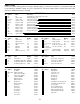
PARTS LIST If you are a student, and any parts are missing or damaged, please see instructor or bookstore. If you purchased this FM receiver kit from a distributor, catalog, etc., please contact Elenco Electronics (address/phone/e-mail is at the back of this manual) for additional assistance, if needed. TM RESISTORS Qty. 1 1 2 2 2 1 1 1 1 1 1 2 Symbol R9 R15 R10, R12 R3, R7 R4, R6 R8 R11 R5 R2 R1 VR2 VR1, VR3 Value 0Ω 10Ω 5% 1/4W 1kΩ 5% 1/4W 3.3kΩ 5% 1/4W 4.7kΩ 5% 1/4W 8.
THE AR-2N6 3. Specifications and testing procedure for each circuit. It is the goal of this project to educate the builder in all of the principles needed to design and build this kit. The radio is broken down into four blocks. Each block contains: 4. Troubleshooting guide for each circuit. 5. Quiz on circuit (answers included). 1. Explanation of circuit to be assembled (Theory of Operation). A final quiz is included (with answers) to help demonstrate the overall knowledge gained by building this kit.
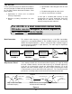
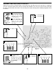
Narrow Band The selectivity of the entire system is limited to only enough frequencies to pass voice or low frequency data. A normal FM receiver would have a bandwidth large enough to pass music and high frequency data transmissions. Narrow Band Wide Bandwidth 3kHz 200kHz Figure 3 FM Radio Receiver The letters “FM” stand for Frequency Modulation. The other popular forms of modulation are AM (Amplitude Modulation) and PM (Phase Modulation).
BLOCK 1 - THE AUDIO AMPLIFIER THEORY OR OPERATION The audio in this radio is amplified by using an integrated circuit audio power amplifier. The LM-386 specifications are as follows: The output impedance of the amplifier is low enough to drive an 8Ω speaker directly. The coupling capacitor value is picked to pass audio signals down to 100 cycles by matching the reactance of the capacitor with the speaker impedance. In other words, 8Ω = 1/2πfC, where f = 100Hz.
ASSEMBLY INSTRUCTIONS FOR BLOCK 1 Solder the parts to the PC board and put a check mark in the box (!) next to each step after it is completed. The parts should be similar to the sketch in each box, but will differ in size. Be sure to check each solder point for shorts and cold solder connections. Be careful to prevent static discharge when handling integrated circuits U2 and U3. Insert the IC socket into the PC board with the notch in the same direction as the marking on the PC board. Notch 104 C3 - .
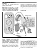
CONNECTING PARTS TO THE BACK SIDE OF THE PC BOARD Twist two leads of a 10Ω resistor and a .047µF capacitor as shown in Figure 8a. Solder the wires close to the components and clip off any excess wire. Solder 473 C22 - .047µF Capacitor (473) R15 - 10Ω Resistor (brown-black-black-gold) Figure 8a Mount the components shown in Figure 8 to the foil side of the PC board. Place a check mark in the box (!) after each part is in place. 502 C2 - .005µF Capacitor (502) C2 - .
CONNECTING THE FRONT PANEL PARTS TO THE PC BOARD Solder the parts to the PC board and put a check mark in the box (!) next to each step after it is completed. The parts should be similar to what is shown in Figure 9. To wire the speaker, pot and switch, cut the indicated length of wire from the roll of 22 gauge solid wire and strip 1/4” of insulation off of each end. Before soldering, mechanically connect the wire to the parts as shown in the figure.
TEST PROCEDURE - BLOCK 1 Procedure 1 If you do not have an audio generator and multimeter, skip to procedure 2. and connect to the circuit as shown in Figure 10. Connect the positive voltage probe to the positive lead of capacitor C4. Connect the common probe to the negative lead from the battery. Turn the power ON. The multimeter should read between 4.5V and 5.5V. If not, turn off the power and check that U3 is correctly installed. Also, check for solder shorts and unsoldered leads.
455kHz V 20A COM A Ω VΩ 9V Battery Figure 11 Power Output Multiply the peak by 0.707 and square the result. Divide by 8Ω (speaker impedance) to obtain the maximum power output before clipping distortion occurs. Maximum power output should be 1/2W or greater. If this test fails, replace the battery with a power supply capable of delivering 1/2A @ 9V or replace the battery with a fresh alkaline battery. If you do not have an audio generator and an oscilloscope, skip this test.
Frequency Response If you do not have an audio generator and an oscilloscope, skip this test. Make sure that the power is OFF and connect the audio generator and the oscilloscope as shown in Figure 11 (replace the multimeter leads with scope leads). Set the generator to 400Hz minimum output and set the oscilloscope to read 1V/div. Put the volume control in the fully clockwise position. Turn the power ON and adjust the audio generator output until a waveform similar to the one shown in Figure 13 is obtained.
Feedback Capacitor 104 9V Battery Volume control in mid-position Figure 14 QUIZ 1 1. The impedance of a 200µF capacitor at 100Hz is: (a) 50Ω (b) 79.6Ω (c) 2Ω (d) 7.96Ω 6. The first IF frequency in the AR-2N6 Radio Kit is: (a) 455kHz (b) 10.7MHz (c) 150MHz (d) 50MHz 2. If the frequency is 150MHz, the wavelength is approximately . . . (a) 20 meters (c) 6 meters (b) 2 meters (d) need more information 7. In order to get the second IF frequency, a crystal oscillator must be set at: (a) 455kHz (c) 10.
BLOCK 2 - RECOVERING THE DATA Theory of Operation In dealing with FM receivers, there are some terms that must be defined. First, let’s determine the term deviation as the frequency swing of the incoming FM signal. When no modulation is present, the incoming signal is a fixed frequency carrier wave (Fc). Positive deviation (Fp) is the increase in Fc due to modulation, and negative deviation (Fn) is the decrease in Fc due to the modulation.
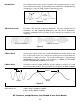
Amplitude Amplitude Lower R Frequency Linear Area Narrow Band Frequency Same Deviation Figure 16 Notice how the linearity improves for a given amount of frequency deviation when the positive and negative peaks are further apart. Figure 16 also shows how the amplitude of the output would drop for the same frequency deviation on a more linear detector. in a synchronous detector.
ASSEMBLY INSTRUCTIONS FOR BLOCK 2 Turn the switch OFF and remove the battery. Solder the parts to the PC board and put a check mark in the box (!) next to each step after it is completed. The parts should be similar to the sketch in each box, but will differ in size. Be sure to check each solder point for shorts and cold solder connections. Be careful to prevent static discharge when handling the integrated circuit U1. 104 C18 - .1µF Capacitor F1 - 455kHz Filter C19 - .1µF Capacitor C20 - .
CONNECTING THE SQUELCH CONTROL TO THE PC BOARD Cut two 3” pieces of wire from the roll of 22 guage soild wire and strip 1/4” of the insulation off of each end. Using these wires, solder the 100kΩ potentiometer (VR1) to the PC board and put a check mark in the box (!) after both wires are in place. This part should be similar to the sketch shown in the box, but may differ in size. Be sure to mechanically connect each wire as shown in Figure 19 before soldering.
TEST PROCEDURE - BLOCK 2 Procedure 3 integrated circuit U1. Connect the common probe to the negative lead from the battery. Turn the power ON. The multimeter should read between 4.5V and 5.5V. If not, turn off the power and check that coil L5 is correctly installed. Also, check for solder shorts, unsoldered leads, or an open copper run between the positive side of C14 and coil L5. If you do not have a multimeter, skip to procedure 4. DC Test Make sure that the power switch is in the OFF position.
AC Test rise to a maximum of about 3.0V, then fall to a minimum of about 1.5V and then rise again. Record the maximum (Vmax) and minimum (Vmin) voltages. Set L5 midway between Vmax and Vmin. For example, if Vmax = 2.95V and Vmin = 1.45V, set L5 to (Vmax + Vmin)/2 = (2.95 + 1.45)/2 = (4.40)/2 = 2.2V. If you do not have a signal generator, skip to procedure 4. Make sure that the power switch is in the OFF position. Turn the squelch control fully counterclockwise .
Squelch Control Check Move the multimeter probe from pin 13 to pin 11 of U1. The voltage should be near 0V. Turn the squelch control clockwise until the voltage jumps to about 2.6V, disabling the audio amplifier. If the voltage does not jump, use a voltage divider to reduce the signal generator output to 5mV peak to peak and try again. If the voltage still does not jump, check the wiring to the squelch control pot. Also, be sure that the temporary jumper installed in block 1 was removed.
QUIZ 2 1. When no FM modulation is present, the incoming signal frequency is . . . (a) DC (b) fixed (c) minimum (d) maximum 6. When the quadrature detector is made more linear by separating the peaks, the output . . . (a) increases (b) remains the same (c) produces more distortion (d) decreases 2. An increase in the carrier frequency due to modulation is called . . . (a) detection (b) negative deviation (c) positive deviation (d) peaking 7.
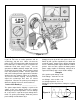
ASSEMBLY INSTRUCTIONS FOR BLOCKS 3 & 4 Turn the switch OFF and remove the battery. Solder the parts to the PC board and put a check mark in the box (!) next to each part after it is installed. The parts should be similar to the sketch in each box, but will differ in size. Be sure to check each solder point for shorts and cold solder connections. 103 C11 - .01µF Capacitor (103) C13 - .01µF Capacitor (103) 102 C10 - .001µF Capacitor (102) C7 - 470pF Capacitor (471) 104 C8 - 7pF Capacitor (7) C9 - .
ASSEMBLY INSTRUCTIONS FOR BLOCKS 3 & 4 (Continued) R9 - 0Ω Jumper Wire R10 - 1kΩ Resistor (brown- black - red - gold) L2 - Turnable Coil L3 - Turnable Coil Use a discarded resistor lead. R4 & R6 - 4.7kΩ Resistor (yellow - violet - red - gold) C5 - 3.9pF Capacitor (3.
FINISHING PC BOARD ASSEMBLY Cut three 3” pieces of wire from the roll of 22 gauge solid wire and strip 1/4” of insulation off of each end. Using these wires, solder the 5kΩ potentiometer (VR2) to the PC board and put a check mark in the box (!) after all of the wires are in place. This part should be similar to the sketch shown in the box, but may differ in size. Be sure to mechanically each wire as shown in the figure below before soldering.
CONNECT COMPONENTS TO THE PC BOARD Cut six 1” pieces of 22 gauge wire and strip 1/4” of insulation off of each end. Connect the wires to the remaining DPDT switch as shown in Figure 26a. Insert the six wires into holes F through K and solder to the PC board as shown in Figure 26b. 1/2” Figure 26a Figure 26b FRONT PANEL ASSEMBLY The speaker mounts behind the cluster of holes as shown in Figure 27.
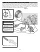
Speaker Phono Jack Nut 4-40 Nuts 4-40 Nut #4 Lockwasher Ground Terminal #4 Lockwashers “L” Bracket “L” Brackets Lockwasher 4-40 Screws (black) Phono Jack Figure 27 Figure 28 Figure 29 -24-
5/16” Internal Tooth Lockwasher Tuning Pot (5kΩ) Volume Pot (100kΩ) Front Panel 2M/6M Switch 2-56 Nuts Flat Washers Squelch Pot 7mm Hex Nut 2-56 Nuts 2-56 Screws On/Off Switch Large Tuning Knob 5/16” Internal Tooth Lockwashers 2-56 Screws 7mm Hex Nuts Volume Knob Squelch Knob Figure 30 Figure 31 -25-
FINAL TEST AND ALIGNMENT More About Squelch Attach a two foot or longer length of wire to the male RCA plug and connect it to the radio antenna jack. Install a fresh battery and turn the power ON. Make sure that the squelch control is fully counterclockwise and the volume control is set at mid-position. A “rushing” noise should be heard from the speaker when no signal is present, which is normal. Slowly tune the radio on each band and listen for activity.
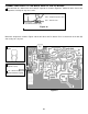
SCHEMATIC DIAGRAM