32” LCD TV chassis FL10.3 SERVICE MANUAL Contents TYPE A LC320EM1 EMERSON (Serial No.: DS1A, DS2A, DS3A, DS4A, DS5A) LC320SL1 SYLVANIA (Serial No.: DS1A, DS2A) LC320SS1 SYLVANIA (Serial No.: DS1A, DS3A) 32MF330B/F7 MAGNAVOX (Serial No.: DS1A, DS3A) 32MF360B/F7 MAGNAVOX (Serial No.: DS1A) TYPE B LC320EM1 EMERSON (Serial No.: DS6A, DS7A, TH1A) LC320SL1 SYLVANIA (Serial No.: DS3A, DS4A, TH1A) LC320EM1F EMERSON (Serial No.: DS1A, DS2A) LC320EM1 EMERSON (Serial No.
IMPORTANT SAFETY NOTICE Proper service and repair is important to the safe, reliable operation of all Funai Equipment. The service procedures recommended by Funai and described in this service manual are effective methods of performing service operations. Some of these service special tools should be used when and as recommended.
TABLE OF CONTENTS Specifications . . . . . . . . . . . . . . . . . . . . . . . . . . . . . . . . . . . . . . . . . . . . . . . . . . . . . . . . . . . . . . . . . . . . . . . . . . . 1-1 Important Safety Precautions . . . . . . . . . . . . . . . . . . . . . . . . . . . . . . . . . . . . . . . . . . . . . . . . . . . . . . . . . . . . . . . 2-1 Standard Notes for Servicing . . . . . . . . . . . . . . . . . . . . . . . . . . . . . . . . . . . . . . . . . . . . . . . . . . . . . . . . . . . . . . .
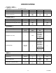
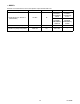
SPECIFICATIONS < TUNER / NTSC > ANT. Input ---------------------- 75 Ω Unbal., F type Description Condition Unit Nominal Limit --- MHz ±2.3 ±2.1 TV.ch.4 CA.ch.31 CA.ch.87 dBµ dBµ dBµ 18 18 18 20 20 23 Condition Unit Nominal Limit --- kHz --- ±100 ch.4 ch.10 ch.41 dBm dBm dBm ------- -76/0 -76/0 -76/+4 Description Condition Unit Nominal Limit 1. Native Pixel Resolution Horizontal Vertical pixels pixels 1366 768 ----- 1. AFT Pull-In Range 2. Synchronizing Sens.
< AUDIO > All items are measured across 8 Ω load at speaker output terminal with L.P.F. Description 1. Audio Output 10% Distortion (ATSC 0 dBfs) 2. Audio Distortion (NTSC) 3. Audio Freq. Response (NTSC) Condition Unit Nominal Limit [LC320EM1, LC320SL1, LC320EM1F] 5.0/5.0 [LC320EM1, LC320SL1, LC320EM1F] 4.5/4.5 [32MF330B/F7, LC320SS1, 32MF360B/F7] 10.0/10.0 [32MF330B/F7, LC320SS1, 32MF360B/F7] 9.0/9.0 Lch/Rch W 500mW: Lch/Rch % 0.5/0.5 2.0/2.
IMPORTANT SAFETY PRECAUTIONS Prior to shipment from the factory, our products are strictly inspected for recognized product safety and electrical codes of the countries in which they are to be sold. However, in order to maintain such compliance, it is equally important to implement the following precautions when a set is being serviced. Safety Precautions for LCD TV Circuit d. Leakage Current Hot Check - With the instrument completely reassembled, plug the AC line cord directly into a 120 V AC outlet.
. Product Safety Notice - Some electrical and mechanical parts have special safety-related characteristics which are often not evident from visual inspection, nor can the protection they give necessarily be obtained by replacing them with components rated for higher voltage, wattage, etc. Parts that have special safety characteristics are identified by a # on schematics and in parts lists.
Precautions during Servicing A. Parts identified by the # symbol are critical for safety. Replace only with part number specified. B. In addition to safety, other parts and assemblies are specified for conformance with regulations applying to spurious radiation. These must also be replaced only with specified replacements. Examples: RF converters, RF cables, noise blocking capacitors, and noise blocking filters, etc. C. Use specified internal wiring.
Safety Check after Servicing Examine the area surrounding the repaired location for damage or deterioration. Observe that screws, parts and wires have been returned to original positions. Afterwards, perform the following tests and confirm the specified values in order to verify compliance with safety standards. 1. Clearance Distance When replacing primary circuit components, confirm specified clearance distance (d) and (d') between soldered terminals, and between terminals and surrounding metallic parts.
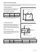
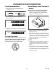
STANDARD NOTES FOR SERVICING Circuit Board Indications How to Remove / Install Flat Pack-IC 1. The output pin of the 3 pin Regulator ICs is indicated as shown. 1. Removal With Hot-Air Flat Pack-IC Desoldering Machine: Top View Out 1. Prepare the hot-air flat pack-IC desoldering machine, then apply hot air to the Flat Pack-IC (about 5 to 6 seconds). (Fig. S-1-1) Bottom View In Input 2. For other ICs, pin 1 and every fifth pin are indicated as shown. 5 Pin 1 10 3.
With Soldering Iron: 3. The flat pack-IC on the CBA is affixed with glue, so be careful not to break or damage the foil of each pin or the solder lands under the IC when removing it. CBA 1. Using desoldering braid, remove the solder from all pins of the flat pack-IC. When you use solder flux which is applied to all pins of the flat pack-IC, you can remove it easily. (Fig.
With Iron Wire: 2. Installation 1. Using desoldering braid, remove the solder from all pins of the flat pack-IC. When you use solder flux which is applied to all pins of the flat pack-IC, you can remove it easily. (Fig. S-1-3) 1. Using desoldering braid, remove the solder from the foil of each pin of the flat pack-IC on the CBA so you can install a replacement flat pack-IC more easily. 2. Affix the wire to a workbench or solid mounting point, as shown in Fig. S-1-5. 2.
Instructions for Handling Semiconductors Electrostatic breakdown of the semi-conductors may occur due to a potential difference caused by electrostatic charge during unpacking or repair work. 1. Ground for Human Body Be sure to wear a grounding band (1 MΩ) that is properly grounded to remove any static electricity that may be charged on the body. 2.
CABINET DISASSEMBLY INSTRUCTIONS [TYPE A, TYPE B] 1. Disassembly Flowchart Removal This flowchart indicates the disassembly steps for the cabinet parts, and the CBA in order to gain access to item(s) to be serviced. When reassembling, follow the steps in reverse order. Bend, route and dress the cables as they were. Step/ Loc. No.
(S-2) (S-4) [2] Rear Cabinet (S-4) (S-2) (S-3) (S-4) (S-2) (S-2) [1] Stand Assembly (S-1) 4-2 Fig. D1 FL10.
[3] Inverter CBA (S-5) (S-7) (S-5) [4] Jack CBA (S-11) (S-6) (S-7) Shield Box (S-7) [5] Power Supply CBA (S-9) [7] Digital Main CBA Unit (S-10) (S-9) (S-8) [6] Jack Holder Fig. D2 4-3 FL10.
[14] Front Cabinet [13] LCD Module Assembly (S-12) Hook [9] Speaker (S-15) [10] Junction CBA [8] Speaker Holder (R) [12] Function CBA (S-14) Hook (S-12) [9] Speaker [11] IR Sensor CBA (S-13) [8] Speaker Holder (L) Fig. D3 4-4 FL10.
TV Cable Wiring Diagram Inverter CBA Jack CBA CN1050 Power Supply CBA CL701B CN1100 CN201 CN1001 CN1150 CL701A CN602 CN302 CN301 CN101 AC CORD CN1900 CN1200 CN1003 CN801 CN802 To LCD Module Assembly To Speaker Digital Main CBA Unit *1 CN3702 *2 CN3006 Junction CBA *1 CN3701 *2 CN3002 *1 CN101 CL102A *2 CN3902 CN3005 IR Sensor CBA Function CBA CL103B CL103C CL101B To LCD Module Assembly *1: TYPE A *2: TYPE B Fig. D4 4-5 FL10.
[TYPE C, TYPE D] 1. Disassembly Flowchart Removal Step/ Loc. No. This flowchart indicates the disassembly steps for the cabinet parts, and the CBA in order to gain access to item(s) to be serviced. When reassembling, follow the steps in reverse order. Bend, route and dress the cables as they were.
(S-2) (S-4) [2] Rear Cabinet (S-4) (S-2) (S-3) (S-4) (S-2) (S-2) [1] Stand Assembly (S-1) 4-7 Fig. D1 FL10.
[3] Inverter CBA (S-5) (S-7) (S-5) [4] Jack CBA (S-11) (S-6) (S-7) Shield Box (S-7) [5] Power Supply CBA (S-9) [7] Digital Main CBA Unit (S-10) (S-9) (S-8) [6] Jack Holder Fig. D2 4-8 FL10.
[13] Front Cabinet [12] LCD Module Assembly (S-12) Hook [9] Speaker (S-15) [8] Speaker Holder (R) [11] Function CBA (S-14) Hook (S-12) [9] Speaker [10] IR Sensor CBA (S-13) [8] Speaker Holder (L) Fig. D3 4-9 FL10.
TV Cable Wiring Diagram Inverter CBA Jack CBA CN1050 Power Supply CBA CL701B CN1100 CN201 CN1001 CN1150 CL701A CN602 CN302 CN301 CN101 AC CORD CN1900 CN1200 CN1003 CN801 CN802 To LCD Module Assembly To Speaker Digital Main CBA Unit CN3006 CN3002 CN3005 IR Sensor CBA Function CBA CL103B CL103C CL101B To LCD Module Assembly Fig. D4 4-10 FL10.
ELECTRICAL ADJUSTMENT INSTRUCTIONS How to set up the service mode: General Note: “CBA” is abbreviation for “Circuit Board Assembly.” Service mode: Note: Electrical adjustments are required after replacing circuit components and certain mechanical parts. It is important to perform these adjustments only after all repairs and replacements have been completed. Also, do not attempt these adjustments unless the proper equipment is available. 1. Turn the power on. 2. Press [MENU] button to display Setup menu.
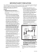
1. Purity Check Mode 2. VCOM Adjustment This mode cycles through full-screen displays of red, green, blue, and white to check for non-active pixels. Test Point Adj. Point 1. Enter the Service mode. Screen 2. Each time pressing [7] button on the remote control unit, the display changes as follows. [CHANNEL UP/DOWN ] buttons M. EQ. Spec. Color analyzer See below Purity Check Mode Figure White mode To avoid interference from ambinent light, this adjustment should be performed in a dark room.
The White Balance Adjustment should be performed when replacing the LCD Panel or Digital Main CBA. Purpose: To mix red, green and blue beams correctly for pure white. 5. [CUTOFF] Press [1] button to select “COR” for Red Cutoff adjustment. Press [3] button to select “COB” for Blue Cutoff adjustment. [DRIVE] Press [4] button to select “DR” for Red Drive adjustment. Press [6] button to select “DB” for Blue Drive adjustment. Symptom of Misadjustment: White becomes bluish or reddish. 6.
HOW TO INITIALIZE THE LCD TV The purpose of initialization is to place the set in a new out of box condition. The customer will be prompted to select a language and program channels after the set has been initialized. To put the program back at the factory-default, initialize the LCD TV using the following procedure. 1. Turn the power on. 2. Enter the service mode. - To cancel the service mode, press [POWER] button on the remote control unit. 3.
FIRMWARE RENEWAL MODE Equipment Required The appearance shown in *1 is described as follows. Appearance a. USB storage device b. Remote Control Unit State Downloading... Downloading the firmware from the USB storage device. Firmware Update Procedure Writing... Writing the downloaded firmware in flash memory. Note: There are two states (the User Upgrade and the Factory Upgrade) in firmware update. Checking... Checking the new firmware. User Upgrade Upgrade the firmware only.
TROUBLESHOOTING [ Power Supply Section ] FLOW CHART NO.1 The power cannot be turned on. No Is the fuse (F601) normal? See FLOW CHART No.2 Yes Is normal state restored when once unplugged power cord is plugged again several seconds? No Yes Is the AL+33V line voltage normal? No Check if there is any leak or short-circuiting on the primary circuit component, and service it if defective.
FLOW CHART NO.6 LCD+24.5V is not output. Is approximately +30V voltage supplied to the collector of Q210? No See FLOW CHART No.5 Yes Check Q207, Q208, D205, P-ON-H1 line and their periphery circuit, and service it if defective. FLOW CHART NO.7 LCD+16V is not output. Is approximately +19.5V voltage supplied to the collector of Q209? No Check C631, D631, D635 and their periphery circuit, and service it if defective.
FLOW CHART NO.10 P-ON+5V is not output. (LCD+16V is outputted normally.) Is approximately +6.8V voltage supplied to the collector of Q641 and the collector of Q643? No See FLOW CHART No.9 Yes Is approximately +6V voltage supplied to the base of Q641 and the base of Q643? No Check D645 and their periphery circuit, and service it if defective. Yes Replace Q641 or Q643. FLOW CHART NO.11 TUNER+5V is not output. (LCD+16V is outputted normally.) Is approximately +6.
FLOW CHART NO.14 P-ON+3.3V is not output. Is approximately +5V voltage supplied to the cathode of D633? No Check C633, D633 and their periphery circuit, and service it if defective. Yes Is the "H" signal (approximately +3.5V) inputted to the base of Q637? No Check Q638, Q639, D666, P-ON-H2 line and their periphery circuit, and service it if defective. Yes Replace Q637. FLOW CHART NO.15 P-ON+9V is not output. (LCD+16V is outputted normally.
[ Video Signal Section ] FLOW CHART NO.1 The key operation is not functioning. Are the contact point and installation state of the key switches (SW101A, SW103A~SW107A) normal? No Re-install the switches (SW101A, SW103A~SW107A) correctly or replace the poor switch. Yes When pressing each switches (SW101A, SW103A~ SW107A) do the voltage of Pin(29) of CN302 increase? No Check the switches (SW101A, SW103A~SW107A) and their periphery circuit, and service it if defective.
FLOW CHART NO.4 Picture does not appear normally.(Tuner input) Are the DIF signal inputted to the Pin(26,28) of CN302? No Yes Check the line between Pin(26, 28) of CN302 and Pin(10, 11) of TU301, and service it if defective. Replace Digital Main CBA Unit or LCD Module Assembly. FLOW CHART NO.5 Picture does not appear normally.(S-Video input) Are the video signal outputted to the Pin(6, 8) of CN302? No Check the line between Pin(6, 8) of CN302 and JK751, and service it if defective.
[ Audio Signal Section ] FLOW CHART NO.1 Audio is not outputted normally.(Audio input) Are the audio(L/R) signals inputted to Pin(2, 15) of IC771? No Check the line between Pin(2, 15) of IC771 and input terminal(JK753, JK754), and service it if defective. Yes Are the audio(L/R) signals inputted to each pin of CN301? Pin(6) : Pin(8) : Pin(2) : Pin(4) : No Replace Digital Main CBA Unit.
FLOW CHART NO.2 Audio is not outputted normally.(Component Audio input) Are the audio(L/R) signals inputted to the Pin(4, 11) of IC771? No Check the line between Pin(4, 11) of IC771 and input terminal(JK741, JK742), and service it if defective. Yes Are the audio(L/R) signals inputted to each pin of CN301? Pin(6) : Pin(8) : Pin(2) : Pin(4) : No Replace Digital Main CBA Unit.
FLOW CHART NO.3 Audio is not outputted normally.(HDMI Audio input) Are the audio(L/R) signals inputted to Pin(5, 14) of IC771? No Check the line between Pin(5, 14) of IC771 and input terminal(JK721, JK722), and service it if defective. Yes Are the audio(L/R) signals inputted to each pin of CN301? Pin(6) : Pin(8) : Pin(2) : Pin(4) : No Replace Digital Main CBA Unit.
FLOW CHART NO.4 Audio is not outputted normally.(Tuner input) Are the DIF signals outputted to the Pin(26, 28) of CN302? No Check TU301 and their periphery circuit, and service it if defective. Yes Are the audio(L/R) signals inputted to each pin of CN301? Pin(6) : Pin(8) : Pin(2) : Pin(4) : No Replace Digital Main CBA Unit.
9-1 SCK SI SO CS WP N2 CLKIN-32K N1 CLKOUT-32K X3102 32.
JK751 S-VIDEO -IN C Y 9-2 CL701B 5 3 1 2 VIDEO-IN S-VIDEO-C-IN S-VIDEO-Y-IN S-VIDEO-SW CL701A 5 3 1 2 DIF-OUT1 12 DIF-OUT2 13 IF-AGC 14 (TUNER UNIT) * TU301 DIF-OUT1 11 DIF-OUT2 10 IF-AGC 9 (TUNER UNIT) * TU301 Either TU301 is used for Power Supply CBA.
JACK CBA 9-3 SP802 SPEAKER R-CH SP801 SPEAKER L-CH JK841 DIGITAL AUDIO-OUT (COAXIAL) CN801 SP(L)+ 2 SP(L)- 1 CN802 SP(R)+ 2 SP(R)- 1 CL801 CL802 BUFFER Q841 MUTE Q873,Q874 DRIVE DRIVE2 35,36 31,32 PWM2 5 3 44 1 Q771 13 3 Q801 Q772 POWER SUPPLY CBA 20 MUTE CONTROL DRIVE1 9,10 13,14 PWM1 IC871 (OP AMP) 9 10 CONTROL LOGIC IC801 (AUDIO AMP) 7 15 11 12 14 2 4 1 5 IC771 (AUDIO SELECTOR) JK872 AUDIO(R)-OUT Q872 MUTE CL701A 7 9 1 Q871 CL701B 7 AUDIO(L)-IN 9 AUDIO(R)-IN JK8
9-4 TMDS-D0(+) TMDS-D0(-) TMDS-D1(+) TMDS-D1(-) TMDS-D2(+) TMDS-D2(-) TMDS-CLOCK(+) TMDS-CLOCK(-) SDA SCL 7 9 4 6 HDMI-IN2 1 3 10 12 16 15 TMDS-D0(+) TMDS-D0(-) TMDS-D1(+) TMDS-D1(-) TMDS-D2(+) TMDS-D2(-) TMDS-CLOCK(+) TMDS-CLOCK(-) SDA SCL JK3704 7 9 4 6 HDMI-IN3 1 3 10 12 16 15 57 56 60 59 63 62 54 53 51 52 8 7 11 10 14 13 5 4 1 2 42 41 45 44 48 47 39 38 36 37 HDMI SW 26 27 23 24 20 21 17 18 A3 A2 B5 A5 C8 B6 A6 J20 J19 J21 J22 H20 A/D CONVERTER P21 P22 N21 N22 M21 M22 L21 L22 VIDEO DECODER
TO SYSTEM CONTROL BLOCK DIAGRAM (CN201) TO POWER SUPPLY BLOCK DIAGRAM (CN602) 10 11 12 2 Q1931 9-5 CN1001 PROTECT3 BACKLIGHT-SW BACKLIGHT-ADJ VCOM COLD HOT Q1932 Q1930 SWITCHING CN1900 2 ACL 1 HOT-GND HOT CIRCUIT. BE CAREFUL. 11 3 15 8 2 3 Q1971 1 4 IC1931 2 3 Q1970 1 4 IC1930 14 7 5 4 10 2 T1950 Q1621 Q1004, Q1005 SW Q1800,Q1815 SW+16V INV+16V Q1972 NOTE: The voltage for parts in hot circuit is measured using hot GND as a common terminal.
TO INVERTER BLOCK DIAGRAM (CN1900) AC601 AC CORD LINE FILTER LINE FILTER 9-6 BRIDGE RECTIFIER D601- D604 POWER SUPPLY CBA Q602 SWITCHING CONTROL L602 L601 Q601 SWITCHING CN602 2 ACL 1 HOT-GND 4A/125V F601 4A/125V HOT CIRCUIT. BE CAREFUL. FEED BACK Q631 19 15 16 13 18 17 12 14 11 COLD 2 3 HOT 1 4 IC601 9 8 7 5 4 3 T601 CAUTION ! Fixed voltage (or Auto voltage selectable) power supply circuit is used in this unit.
9-7 SCK SI SO CS WP DIGITAL MAIN CBA UNIT T22 XIN25 T21 XOUT25 X3001 25MHz OSC SCK SIN SOUT CS WP V19 Y21 AA22 Y20 AA21 H21 G22 H22 AB21 W20 W17 AL+3.
JK751 S-VIDEO -IN C Y 9-8 CL701B 5 3 1 2 VIDEO-IN S-VIDEO-C-IN S-VIDEO-Y-IN S-VIDEO-SW CL701A 5 3 1 2 DIF-OUT1 12 DIF-OUT2 13 IF-AGC 14 (TUNER UNIT) * TU301 DIF-OUT1 11 DIF-OUT2 10 IF-AGC 9 (TUNER UNIT) * TU301 Either TU301 is used for Power Supply CBA.
JACK CBA 9-9 SP802 SPEAKER R-CH SP801 SPEAKER L-CH JK841 DIGITAL AUDIO-OUT (COAXIAL) CN801 SP(L)+ 2 SP(L)- 1 CN802 SP(R)+ 2 SP(R)- 1 CL801 CL802 BUFFER Q841 MUTE Q873,Q874 DRIVE DRIVE2 35,36 31,32 PWM2 5 3 44 1 Q771 13 3 Q801 Q772 POWER SUPPLY CBA 20 MUTE CONTROL DRIVE1 9,10 13,14 PWM1 IC871 (OP AMP) 9 10 CONTROL LOGIC IC801 (AUDIO AMP) 7 15 11 12 14 2 4 1 5 IC771 (AUDIO SELECTOR) JK872 AUDIO(R)-OUT Q872 MUTE CL701A 7 9 1 Q871 CL701B 7 AUDIO(L)-IN 9 AUDIO(R)-IN JK8
9-10 TMDS-D0(+) TMDS-D0(-) TMDS-D1(+) TMDS-D1(-) TMDS-D2(+) TMDS-D2(-) TMDS-CLOCK(+) TMDS-CLOCK(-) SDA Q3016 SCL BUFFER 7 9 4 6 HDMI-IN3 1 3 10 12 16 15 TMDS-D0(+) TMDS-D0(-) TMDS-D1(+) TMDS-D1(-) TMDS-D2(+) TMDS-D2(-) TMDS-CLOCK(+) TMDS-CLOCK(-) SDA Q3017 SCL BUFFER JK3002 7 9 4 6 HDMI-IN2 1 3 10 12 16 15 Q3019 BUFFER Q3018 BUFFER Q3020 BUFFER AUDIO(L) AUDIO(R) SPDIF AMP(L)-OUT AMP(R)-OUT BCLK LRCLK ACLK ADATA IF-AGC S-VIDEO-SW DIF-OUT1 DIF-OUT2 TMDS-D0(+) TMDS-D0(-) TMDS-D1(+) TMDS-D1(-) TM
TO SYSTEM CONTROL BLOCK DIAGRAM (CN201) TO POWER SUPPLY BLOCK DIAGRAM (CN602) 10 11 12 2 Q1931 9-11 CN1001 PROTECT3 BACKLIGHT-SW BACKLIGHT-ADJ VCOM COLD HOT Q1932 Q1930 SWITCHING CN1900 2 ACL 1 HOT-GND HOT CIRCUIT. BE CAREFUL. 11 3 15 8 2 3 Q1971 1 4 IC1931 2 3 Q1970 1 4 IC1930 14 7 5 4 10 2 T1950 Q1621 Q1004, Q1005 SW Q1800,Q1815 SW+16V INV+16V Q1972 NOTE: The voltage for parts in hot circuit is measured using hot GND as a common terminal.
TO INVERTER BLOCK DIAGRAM (CN1900) AC601 AC CORD LINE FILTER LINE FILTER 9-12 BRIDGE RECTIFIER D601- D604 POWER SUPPLY CBA Q602 SWITCHING CONTROL L602 L601 Q601 SWITCHING CN602 2 ACL 1 HOT-GND 4A/125V F601 4A/125V HOT CIRCUIT. BE CAREFUL. FEED BACK Q631 19 15 16 13 18 17 12 14 11 COLD 2 3 HOT 1 4 IC601 9 8 7 5 4 3 T601 CAUTION ! Fixed voltage (or Auto voltage selectable) power supply circuit is used in this unit.
9-13 SCK SIN SOUT CS WP T22 XIN25 T21 XOUT25 V19 Y21 AA22 Y20 AA21 H21 G22 H22 AB21 W20 W17 AL+3.
JK751 S-VIDEO -IN C Y 9-14 CL701B 5 3 1 2 VIDEO-IN S-VIDEO-C-IN S-VIDEO-Y-IN S-VIDEO-SW CL701A 5 3 1 2 DIF-OUT1 12 DIF-OUT2 13 IF-AGC 14 (TUNER UNIT) * TU301 DIF-OUT1 11 DIF-OUT2 10 IF-AGC 9 (TUNER UNIT) * TU301 Either TU301 is used for Power Supply CBA.
JACK CBA 9-15 SP802 SPEAKER R-CH SP801 SPEAKER L-CH JK841 DIGITAL AUDIO-OUT (COAXIAL) CN801 SP(L)+ 2 SP(L)- 1 CN802 SP(R)+ 2 SP(R)- 1 CL801 CL802 BUFFER Q841 MUTE Q873,Q874 DRIVE DRIVE2 35,36 31,32 PWM2 5 3 44 1 Q771 13 3 Q801 Q772 POWER SUPPLY CBA 20 MUTE CONTROL DRIVE1 9,10 13,14 PWM1 IC871 (OP AMP) 9 10 CONTROL LOGIC IC801 (AUDIO AMP) 7 15 11 12 14 2 4 1 5 IC771 (AUDIO SELECTOR) JK872 AUDIO(R)-OUT Q872 MUTE CL701A 7 9 1 Q871 CL701B 7 AUDIO(L)-IN 9 AUDIO(R)-IN JK
9-16 TMDS-D0(+) TMDS-D0(-) TMDS-D1(+) TMDS-D1(-) TMDS-D2(+) TMDS-D2(-) TMDS-CLOCK(+) TMDS-CLOCK(-) SDA Q3016 SCL BUFFER 7 9 4 6 HDMI-IN3 1 3 10 12 16 15 TMDS-D0(+) TMDS-D0(-) TMDS-D1(+) TMDS-D1(-) TMDS-D2(+) TMDS-D2(-) TMDS-CLOCK(+) TMDS-CLOCK(-) SDA Q3017 SCL BUFFER JK3002 7 9 4 6 HDMI-IN2 1 3 10 12 16 15 Q3019 BUFFER Q3018 BUFFER Q3020 BUFFER AUDIO(L) AUDIO(R) SPDIF AMP(L)-OUT AMP(R)-OUT BCLK LRCLK ACLK ADATA IF-AGC S-VIDEO-SW DIF-OUT1 DIF-OUT2 TMDS-D0(+) TMDS-D0(-) TMDS-D1(+) TMDS-D1(-) TM
TO SYSTEM CONTROL BLOCK DIAGRAM (CN201) TO POWER SUPPLY BLOCK DIAGRAM (CN602) 10 11 12 2 Q1931 9-17 CN1001 PROTECT3 BACKLIGHT-SW BACKLIGHT-ADJ VCOM COLD HOT Q1932 Q1930 SWITCHING CN1900 2 ACL 1 HOT-GND HOT CIRCUIT. BE CAREFUL. 11 3 15 8 2 3 Q1971 1 4 IC1931 2 3 Q1970 1 4 IC1930 14 7 5 4 10 2 T1950 Q1621 Q1004, Q1005 SW Q1800,Q1815 SW+16V INV+16V Q1972 NOTE: The voltage for parts in hot circuit is measured using hot GND as a common terminal.
TO INVERTER BLOCK DIAGRAM (CN1900) AC601 AC CORD LINE FILTER LINE FILTER 9-18 BRIDGE RECTIFIER D601- D604 POWER SUPPLY CBA Q602 SWITCHING CONTROL L602 L601 Q601 SWITCHING CN602 2 ACL 1 HOT-GND 4A/125V F601 4A/125V HOT CIRCUIT. BE CAREFUL. FEED BACK Q631 19 15 16 13 18 17 12 14 11 COLD 2 3 HOT 1 4 IC601 9 8 7 5 4 3 T601 CAUTION ! Fixed voltage (or Auto voltage selectable) power supply circuit is used in this unit.
SCHEMATIC DIAGRAMS / CBA AND TEST POINTS Standard Notes WARNING Many electrical and mechanical parts in this chassis have special characteristics. These characteristics often pass unnoticed and the protection afforded by them cannot necessarily be obtained by using replacement components rated for higher voltage, wattage, etc.
LIST OF CAUTION, NOTES, AND SYMBOLS USED IN THE SCHEMATIC DIAGRAMS ON THE FOLLOWING PAGES: 1. CAUTION: CAUTION: FOR CONTINUED PROTECTION AGAINST RISK OF FIRE, REPLACE ONLY WITH SAME TYPE_A,_V FUSE. ATTENTION: UTILISER UN FUSIBLE DE RECHANGE DE MÊME TYPE DE_A,_V. 2. CAUTION: Fixed Voltage (or Auto voltage selectable) power supply circuit is used in this unit.
Power Supply 1 Schematic Diagram CAUTION ! Fixed voltage (or Auto voltage selectable) power supply circuit is used in this unit. If Main Fuse (F601) is blown , check to see that all components in the power supply circuit are not defective before you connect the AC plug to the AC power supply. Otherwise it may cause some components in the power supply circuit to fail. 4A/125V CAUTION ! : For continued protection against risk of fire, replace only with same type 4 A, 125V fuse.
Power Supply 2 Schematic Diagram 10-4 FL10.
Power Supply 3 & Jack Schematic Diagram 10-5 FL10.
Power Supply 4 Schematic Diagram 10-6 FL10.
Inverter Schematic Diagram NOTE: The voltage for parts in hot circuit is measured using hot GND as a common terminal. 10-7 FL10.
Function Schematic Diagram 10-8 FL10.
IR Sensor & Junction Schematic Diagram 10-9 FL10.
Digital Main 1 Schematic Diagram [TYPE A] 1 NOTE: The order of pins shown in this diagram is different from that of actual IC3301. IC3301 is divided into five and shown as IC3301 (1/6) ~ IC3301 (6/6) in this Digital Main Schematic Diagram Section. 10-10 FL10.
Digital Main 2 Schematic Diagram [TYPE A] 1 NOTE: The order of pins shown in this diagram is different from that of actual IC3301. IC3301 is divided into five and shown as IC3301 (1/6) ~ IC3301 (6/6) in this Digital Main Schematic Diagram Section. 10-11 FL10.
Digital Main 3 Schematic Diagram [TYPE A] 1 NOTE: The order of pins shown in this diagram is different from that of actual IC3301. IC3301 is divided into five and shown as IC3301 (1/6) ~ IC3301 (6/6) in this Digital Main Schematic Diagram Section. 10-12 FL10.
Digital Main 4 Schematic Diagram [TYPE A] 1 NOTE: The order of pins shown in this diagram is different from that of actual IC3301. IC3301 is divided into five and shown as IC3301 (1/6) ~ IC3301 (6/6) in this Digital Main Schematic Diagram Section. 10-13 FL10.
Digital Main 5 Schematic Diagram [TYPE A] 1 NOTE: The order of pins shown in this diagram is different from that of actual IC3301. IC3301 is divided into five and shown as IC3301 (1/6) ~ IC3301 (6/6) in this Digital Main Schematic Diagram Section. 10-14 FL10.
Digital Main 6 Schematic Diagram [TYPE A] 1 NOTE: The order of pins shown in this diagram is different from that of actual IC3301. IC3301 is divided into five and shown as IC3301 (1/6) ~ IC3301 (6/6) in this Digital Main Schematic Diagram Section. 10-15 FL10.
Digital Main 1 Schematic Diagram [TYPE B, TYPE C, TYPE D] 1 NOTE: The order of pins shown in this diagram is different from that of actual IC3005. IC3005 is divided into five and shown as IC3005 (1/6) ~ IC3005 (6/6) in this Digital Main Schematic Diagram Section. 10-16 FL10.
Digital Main 2 Schematic Diagram [TYPE B, TYPE C, TYPE D] 1 NOTE: The order of pins shown in this diagram is different from that of actual IC3005. IC3005 is divided into five and shown as IC3005 (1/6) ~ IC3005 (6/6) in this Digital Main Schematic Diagram Section. 10-17 FL10.
Digital Main 3 Schematic Diagram [TYPE B, TYPE C, TYPE D] 1 NOTE: The order of pins shown in this diagram is different from that of actual IC3005. IC3005 is divided into five and shown as IC3005 (1/6) ~ IC3005 (6/6) in this Digital Main Schematic Diagram Section. 10-18 FL10.
Digital Main 4 Schematic Diagram [TYPE B, TYPE C, TYPE D] 1 NOTE: The order of pins shown in this diagram is different from that of actual IC3005. IC3005 is divided into five and shown as IC3005 (1/6) ~ IC3005 (6/6) in this Digital Main Schematic Diagram Section. 10-19 FL10.
Digital Main 5 Schematic Diagram [TYPE B, TYPE C, TYPE D] 1 NOTE: The order of pins shown in this diagram is different from that of actual IC3005. IC3005 is divided into five and shown as IC3005 (1/6) ~ IC3005 (6/6) in this Digital Main Schematic Diagram Section. 10-20 FL10.
Digital Main 6 Schematic Diagram [TYPE B, TYPE C, TYPE D] 1 NOTE: The order of pins shown in this diagram is different from that of actual IC3005. IC3005 is divided into five and shown as IC3005 (1/6) ~ IC3005 (6/6) in this Digital Main Schematic Diagram Section. 10-21 FL10.
Power Supply CBA & Jack CBA Top View [TYPE A, TYPE B, TYPE D] CAUTION ! Fixed voltage (or Auto voltage selectable) power supply circuit is used in this unit. If Main Fuse (F601) is blown , check to see that all components in the power supply circuit are not defective before you connect the AC plug to the AC power supply. Otherwise it may cause some components in the power supply circuit to fail.
Power Supply CBA & Jack CBA Bottom View [TYPE A, TYPE B, TYPE D] C902 R902 R903 C903 R752 C755 C757 R761 C761 C758 R762 C762 R754 C754 C756 R698 R662 C752 R756 R758 C751 R757 C753 R760 R753 R759 R755 JK754 C919 R927 R921 JK751 R751 JK752 C914 C917 Q904 R907 C906 L901 Q633 R406 J308 R407 C905 R908 R920 Q903 J318 GND C907 C904 R905 R919 Q401 D420 R665 C402 Q635 R684 R906 R904 R901 C901 D658 R664 R663 R660 R409 J316 R405 R240 R225 Q207 R226 R212 R211 D405
Power Supply CBA & Jack CBA Top View [TYPE C] CAUTION ! Fixed voltage (or Auto voltage selectable) power supply circuit is used in this unit. If Main Fuse (F601) is blown , check to see that all components in the power supply circuit are not defective before you connect the AC plug to the AC power supply. Otherwise it may cause some components in the power supply circuit to fail. 3.5Vfor1.
Power Supply CBA & Jack CBA Bottom View [TYPE C] Power Supply CBA C902 R902 R903 C903 R752 C755 C757 R761 C761 C758 R762 C762 R754 C754 C756 R698 R662 C752 R756 R758 C751 R757 C753 R760 R753 R759 R755 JK754 C919 R927 R921 JK751 R751 JK752 C914 C917 Q904 R907 C906 L901 Q633 R406 J308 R407 C905 R908 R920 Q903 J318 GND C907 C904 R905 R919 Q635 R684 R906 R904 R901 C901 D658 R665 C402 D420 R225 Q207 R226 D405 R910 R911 J326 R636 D648 D649 R231 D204 D406
Inverter CBA, Function CBA, IR Sensor CBA & Junction CBA Top View [TYPE A, TYPE B, TYPE D] NOTE: The voltage for parts in hot circuit is measured using hot GND as a common terminal. Because a hot chassis ground is present in the power supply circuit, an isolation transformer must be used when repairing. Also, in order to have the ability to increase the input slowly, when troubleshooting this type of power supply circuit, a variable isolation transformer is required.
VOL DOWN VOL UP MENU CH DOWN CH UP EJECT STOP PLAY POWER C1062 C1112 C1116 C1162 C1054 J1124 J1125 J1126 J1127 BC1501 BC1500 J1123 J1122 C1205 D1062 D1063 J1105 J1106 J1107 J1108 R1060 GND R1063 R1065 D1065 D1073 R1062 D1074 D1067 D1068 J1093 C1068 D1064 R1061 R1114 R1115 R1064 C1064 D1071 D1211 D1212 D1217 J1088 D1218 D1115 R1113 Q1110 C1114 Q1061 D1070 D1112 R1110 R1214 C1214 48 46 R19 R19 C1940 J1081 J1080 R1050 J1077 J1076 J1085 J1089 R1072 R1071
Inverter CBA, Function CBA & IR Sensor CBA Top View [TYPE C] Because a hot chassis ground is present in the power supply circuit, an isolation transformer must be used when repairing. Also, in order to have the ability to increase the input slowly, when troubleshooting this type of power supply circuit, a variable isolation transformer is required. BA01F4F0103 2 C1065 A3 BA01F4F0103 2 D CN1150 C1115 CN101 6 7 8 9 10 J103 CL103A C101 C7A3 C C1111 C1061 CL102A CL101B D106 TOOL NO.
VOL DOWN VOL UP MENU CH DOWN CH UP EJECT STOP PLAY POWER J102 C1062 C1112 C1116 C1162 C1166 C1212 C1054 J1124 J1125 J1126 J1127 BC1500 BC1501 J1123 J1122 C1205 D1062 D1063 J1105 J1106 J1107 J1108 R1060 GND R1063 R1065 D1065 D1073 R1062 D1074 D1067 D1068 J1093 C1068 D1064 R1115 R1114 D1115 R1113 Q1110 C1114 Q1061 D1070 D1112 R1110 R1214 C1214 R1031 C1011 R1030 D1123 R1112 D1113 J1073 D1111 D1110 R1008 D1114 R1111 R1007 C1004 R1009 D1116 Q1111 C1117 R1116
WAVEFORMS WF1 ~ WF7 = Waveforms to be observed at Waveform check points. (Shown in Schematic Diagram.) Input: NTSC Color Bar Signal (with 1kHz Audio Signal) WF1 Pin 4 of CN302 CVBS WF2 0.2V WF6 20µs 0.2V 20µs AUDIO 0.2V 20µs Pin 19 of CN302 VIDEO-Pr WF7 0.2V Pin 17 of CN302 VIDEO-Pb Pin 6 of CN302 S-VIDEO-C WF4 20µs Pin 8 of CN302 S-VIDEO-Y WF3 WF5 0.2V 20µs Pin 13 of CN302 0.1V 0.5ms Pin 15 of CN302 VIDEO-Y 0.
12-1 AC601 AC CORD WITH PC INPUT PC-AUDIO -IN AUDIO(R) -OUT AUDIO(L) -OUT DIGITAL AUDIO-OUT (COAXIAL) HDMIAUDIO(R)-IN HDMIAUDIO(L)-IN COMPONENTAUDIO(R)-IN CN3702 1 2 3 4 5 6 7 8 9 10 11 12 13 14 15 16 17 18 19 20 21 22 23 24 25 26 27 28 29 CL3702 GND SPDIF GND VIDEO-IN S-VIDEO-SW S-VIDEO-C-IN GND S-VIDEO-Y-IN GND INPUT1 AUDIO(R) INPUT0 AUDIO(L) GND COM-VIDEO-Y-IN GND COM-VIDEO-Pb-IN GND COM-VIDEO-Pr-IN AUDIO-MUTE SDA SCL RESET IF-AGC GND DIF-OUT1 GND DIF-OUT2 KEY-IN1 CN302 1 2 3 4 5 6 7 8 9 10 1
12-2 AC601 AC CORD WITH PC INPUT PC-AUDIO -IN AUDIO(R) -OUT AUDIO(L) -OUT DIGITAL AUDIO-OUT (COAXIAL) HDMIAUDIO(R)-IN HDMIAUDIO(L)-IN COMPONENTAUDIO(R)-IN COMPONENTAUDIO(L)-IN COMPONENT -Pr-IN COMPONENT -Pb-IN COMPONENT -Y-IN CL3702 GND SPDIF GND VIDEO-IN S-VIDEO-SW S-VIDEO-C-IN GND S-VIDEO-Y-IN GND INPUT1 AUDIO(R) INPUT0 AUDIO(L) GND COM-VIDEO-Y-IN GND COM-VIDEO-Pb-IN GND COM-VIDEO-Pr-IN AUDIO-MUTE SDA SCL RESET IF-AGC GND DIF-OUT1 GND DIF-OUT2 KEY-IN1 CN302 1 2 3 4 5 6 7 8 9 10 11 12 13 14
12-3 AC601 AC CORD WITH PC INPUT PC-AUDIO -IN AUDIO(R) -OUT AUDIO(L) -OUT DIGITAL AUDIO-OUT (COAXIAL) HDMIAUDIO(R)-IN HDMIAUDIO(L)-IN COMPONENTAUDIO(R)-IN COMPONENTAUDIO(L)-IN COMPONENT -Pr-IN COMPONENT -Pb-IN COMPONENT -Y-IN CL3702 GND SPDIF GND VIDEO-IN S-VIDEO-SW S-VIDEO-C-IN GND S-VIDEO-Y-IN GND INPUT1 AUDIO(R) INPUT0 AUDIO(L) GND COM-VIDEO-Y-IN GND COM-VIDEO-Pb-IN GND COM-VIDEO-Pr-IN AUDIO-MUTE SDA SCL RESET IF-AGC GND DIF-OUT1 GND DIF-OUT2 KEY-IN1 CN302 1 2 3 4 5 6 7 8 9 10 11 12 13 14
EXPLODED VIEWS Cabinet *2: 32MF330B/F7, LC320SS1, 32MF360B/F7 A12 *2 *1: LC320EM1, LC320SL1, LC320EM1F B15 A15 B15 A1 L2 *1 B5 B15 L2 L2 B4 CL201 A8 SP801 B15 A2 L2 L1 S5 L8 B9 *3 A5 L2 Inverter CBA CL801 A6 B13 L2 L1 Function CBA Junction CBA L16 A10 L3 L2 CL101 CL802 L2 B13 L3 CL103 L2 SP802 L16 L8 IR Sensor CBA L1 L7 B14 CL1003 L8 B8 L1 L1 L16 L1 *3: TYPE A, TYPE B A11 CL701 L1 S5 Jack CBA LCD1 CL3902 L3 B11 L8 Stand Assembly L8 L8 L8 Power Supply C
Packing Some Ref. Numbers are not in sequence. X2 X8 X6 Stand Assembly S2 X10 Packing Tape S5 S9 S6 Tape X1 S2 S3 Packing Tape S4 L9 X3 Tape S3 X4 S1 Packing Tape FR ON FR ON T T S1 S5 13-2 FL10.
PARTS LIST [LC320EM1 (Serial No. : DS1A)] Mechanical Parts PRODUCT SAFETY NOTE: Products marked with a # have special characteristics important to safety. Before replacing any of these components, read carefully the product safety notice in this service manual. Don't degrade the safety of the product through improper servicing. Ref. No. Description Part No.
Electrical Parts PRODUCT SAFETY NOTE: Products marked with a # have special characteristics important to safety. Before replacing any of these components, read carefully the product safety notice in this service manual. Don't degrade the safety of the product through improper servicing. Ref. No. C602# NOTES: 1. Parts that are not assigned part numbers (---------) are not available. 2. Tolerance of Capacitors and Resistors are noted with the following symbols. C.....±0.25% D.....±0.5% F.....±1% G.....
Ref. No. Description C819 ELECTROLYTIC CAP. 10µF/50V M C820 C821 Part No. Ref. No. Description Part No. CE1JMASDL100 D303 DIODE ZENER 5V6BSB-T26 NDTB5R6BST26 CHIP CERAMIC CAP.(1608) B K 1µF/25V CHD1EK30B105 D404 SWITCHING DIODE 1SS133(T-77) QDTZ001SS133 CHIP CERAMIC CAP.(1608) B K 0.1µF/25V CHD1EK30B104 D405 SWITCHING DIODE 1SS133(T-77) QDTZ001SS133 C822 CHIP CERAMIC CAP.(1608) CH J 1000pF/50V CHD1JJ3CH102 D406 DIODE ZENER 15BSB-T26 NDTB015BST26 C823 ELECTROLYTIC CAP.
Ref. No. Description Part No. D806 SWITCHING DIODE 1SS133(T-77) IC201 IC TL3472CDR NSZBA0TTY115 Ref. No. QDTZ001SS133 ICS Description Part No. R204 RES CARBON FILM T 1/4W J 560 Ω R206 CHIP RES. 1/10W J 1k Ω RRXAJR5Z0102 R207 CHIP RES. 1/10W J 100k Ω RRXAJR5Z0104 RCX4561T1001 IC601# PHOTO COUPLER LTV817MCF NPECLTV817MF R208 CHIP RES.
Ref. No. R618 Description RES CARBON FILM T 1/4W J 390k Ω Ref. No. Part No. Description Part No. RCX4394T1001 R743 CHIP RES. 1/10W J 15k Ω RRXAJR5Z0153 R636 RES. CARBON FILM J 1/2W J 2.7 Ω RCX22R7T1003 R744 CHIP RES. 1/10W J 15k Ω RRXAJR5Z0153 R637 RES CARBON FILM T 1/4W J 1.5k Ω RCX4152T1001 R745 CHIP RES. 1/10W J 39k Ω RRXAJR5Z0393 R638 RES CARBON FILM T 1/4W J 1.5k Ω RCX4152T1001 R746 CHIP RES. 1/10W J 39k Ω RRXAJR5Z0393 R639 RES CARBON FILM T 1/4W J 1.
Ref. No. Description Part No. F601# FUSE STC4A125V U/CT PAGE20CW3402 FH601 FUSE HOLDER MSF-015 LF (B110) XH01Z00LY002 INVERTER ASSEMBLY Ref. No.
Ref. No. C1213 Description ELECTROLYTIC CAP. 10µF/50V M Part No. Ref. No. Description Part No. CE1JMASDL100 D1073 SWITCHING DIODE 1SS133(T-77) QDTZ001SS133 C1214 CHIP CERAMIC CAP.(1608) B K 0.01µF/50V CHD1JK30B103 D1074 SWITCHING DIODE 1SS133(T-77) QDTZ001SS133 C1215 CAP CERAMIC HV 15pF/6.3KV/SL/J CCA1500MR001 D1110 SWITCHING DIODE 1SS133(T-77) QDTZ001SS133 C1216 CAP CERAMIC (AX) 1500pF/50V/B/K CA1J152TU061 D1111 SWITCHING DIODE 1SS133(T-77) QDTZ001SS133 C1217 ELECTROLYTIC CAP.
Ref. No. D1972 Description SWITCHING DIODE 1SS133(T-77) Part No. Ref. No. QDTZ001SS133 R1018 Description Part No. RES CARBON FILM T 1/4W J 2.2k Ω RCX4222T1001 D1973 SWITCHING DIODE 1SS133(T-77) QDTZ001SS133 R1019 WIRE COPPER 6111-06003-0120 XZ40C0SHG002 D1990 DIODE FAST RECOVERY 31DF4-FC QDWZ031DF4FC R1021 RES CARBON FILM T 1/4W J 10k Ω RCX4103T1001 D1994 DIODE ZENER 1ZB100BB NDWZ001ZB100 R1022 CHIP RES. 1/10W F 2.2k Ω RRXAFR5H2201 R1023 CHIP RES. 1/10W F 3.
Ref. No. Description R1211 CHIP RES. 1/10W J 20k Ω R1212 R1213 Ref. No. Part No. Description Part No. RES CARBON FILM T 1/4W J 3.9k Ω RCX4392T1001 R1969 RES CARBON FILM T 1/4W J 3.9k Ω RCX4392T1001 R1970 RES CARBON FILM T 1/4W J 270 Ω RCX4271T1001 RRXAFR5H8201 R1971 RES CARBON FILM T 1/4W J 3.9k Ω RCX4392T1001 RES CARBON FILM T 1/4W J 27k Ω RCX4273T1001 R1972 CHIP RES. 1/10W J 68k Ω RRXAJR5Z0683 R1216 CHIP RES. 1/10W J 100k Ω RRXAJR5Z0104 R1973 CHIP RES.
IR SENSOR CBA Ref. No. Description IR SENSOR CBA Consists of the following: Part No. ---------- CAPACITORS C113 ELECTROLYTIC CAP. 47µF/16V M H7 CE1CMAVSL470 C115 CHIP CERAMIC CAP. CH J 330pF/50V CHD1JJ3CH331 D104 LED GREEN 333GT/E(FNA) NPWZ33GTEFNA D105 LED L-53HT NP4Z000L53HT R123 RES CARBON FILM T 1/4W J 220 Ω RCX4221T1001 R124 RES CARBON FILM T 1/4W J 220 Ω RCX4221T1001 R126 CHIP RES. 1/10W J 1k Ω RRXAJR5Z0102 R127 RES CARBON FILM T 1/4W J 3.
PARTS LIST [LC320EM1 (Serial No. : DS2A)] Mechanical Parts PRODUCT SAFETY NOTE: Products marked with a # have special characteristics important to safety. Before replacing any of these components, read carefully the product safety notice in this service manual. Don't degrade the safety of the product through improper servicing. NOTE: Parts that are not assigned part numbers (---------) are not available. Different parts from the original model LC320EM1 (Serial No. : DS1A) Ref. No.
Electrical Parts PRODUCT SAFETY NOTE: Products marked with a # have special characteristics important to safety. Before replacing any of these components, read carefully the product safety notice in this service manual. Don't degrade the safety of the product through improper servicing. NOTES: 1. Parts that are not assigned part numbers (---------) are not available. 2. Tolerance of Capacitors and Resistors are noted with the following symbols. C.....±0.25% D.....±0.5% F.....±1% G.....±2% J......±5% K.
PARTS LIST [LC320EM1 (Serial No. : DS5A)] Mechanical Parts PRODUCT SAFETY NOTE: Products marked with a # have special characteristics important to safety. Before replacing any of these components, read carefully the product safety notice in this service manual. Don't degrade the safety of the product through improper servicing. NOTE: Parts that are not assigned part numbers (---------) are not available. Different parts from the original model LC320EM1 (Serial No. : DS1A) Ref. No. Description Part No.
Electrical Parts PRODUCT SAFETY NOTE: Products marked with a # have special characteristics important to safety. Before replacing any of these components, read carefully the product safety notice in this service manual. Don't degrade the safety of the product through improper servicing. NOTES: 1. Parts that are not assigned part numbers (---------) are not available. 2. Tolerance of Capacitors and Resistors are noted with the following symbols. C.....±0.25% D.....±0.5% F.....±1% G.....±2% J......±5% K.
PARTS LIST [LC320EM1 (Serial No. : DS6A)] Mechanical Parts PRODUCT SAFETY NOTE: Products marked with a # have special characteristics important to safety. Before replacing any of these components, read carefully the product safety notice in this service manual. Don't degrade the safety of the product through improper servicing. NOTE: Parts that are not assigned part numbers (---------) are not available. Different parts from the original model LC320EM1 (Serial No. : DS1A) Ref. No. Description Part No.
Electrical Parts PRODUCT SAFETY NOTE: Products marked with a # have special characteristics important to safety. Before replacing any of these components, read carefully the product safety notice in this service manual. Don't degrade the safety of the product through improper servicing. NOTES: 1. Parts that are not assigned part numbers (---------) are not available. 2. Tolerance of Capacitors and Resistors are noted with the following symbols. C.....±0.25% D.....±0.5% F.....±1% G.....±2% J......±5% K.
PARTS LIST [LC320EM1 (Serial No. : TH1A)] Mechanical Parts PRODUCT SAFETY NOTE: Products marked with a # have special characteristics important to safety. Before replacing any of these components, read carefully the product safety notice in this service manual. Don't degrade the safety of the product through improper servicing. NOTE: Parts that are not assigned part numbers (---------) are not available. Different parts from the original model LC320EM1 (Serial No. : DS1A) Ref. No. Description Part No.
Electrical Parts PRODUCT SAFETY NOTE: Products marked with a # have special characteristics important to safety. Before replacing any of these components, read carefully the product safety notice in this service manual. Don't degrade the safety of the product through improper servicing. NOTES: 1. Parts that are not assigned part numbers (---------) are not available. 2. Tolerance of Capacitors and Resistors are noted with the following symbols. C.....±0.25% D.....±0.5% F.....±1% G.....±2% J......±5% K.
PARTS LIST [LC320EM1 (Serial No. : TH2A)] Mechanical Parts PRODUCT SAFETY NOTE: Products marked with a # have special characteristics important to safety. Before replacing any of these components, read carefully the product safety notice in this service manual. Don't degrade the safety of the product through improper servicing. NOTE: Parts that are not assigned part numbers (---------) are not available. Different parts from the original model LC320EM1 (Serial No. : DS1A) Ref. No. Description Part No.
Electrical Parts PRODUCT SAFETY NOTE: Products marked with a # have special characteristics important to safety. Before replacing any of these components, read carefully the product safety notice in this service manual. Don't degrade the safety of the product through improper servicing. NOTES: 1. Parts that are not assigned part numbers (---------) are not available. 2. Tolerance of Capacitors and Resistors are noted with the following symbols. C.....±0.25% D.....±0.5% F.....±1% G.....±2% J......±5% K.
PARTS LIST [LC320SL1 (Serial No. : DS1A)] Mechanical Parts PRODUCT SAFETY NOTE: Products marked with a # have special characteristics important to safety. Before replacing any of these components, read carefully the product safety notice in this service manual. Don't degrade the safety of the product through improper servicing. NOTE: Parts that are not assigned part numbers (---------) are not available. Different parts from the original model LC320EM1 (Serial No. : DS1A) Ref. No. Description Part No.
Electrical Parts PRODUCT SAFETY NOTE: Products marked with a # have special characteristics important to safety. Before replacing any of these components, read carefully the product safety notice in this service manual. Don't degrade the safety of the product through improper servicing. NOTE: Parts that are not assigned part numbers (---------) are not available. Different parts from the original model LC320EM1 (Serial No. : DS1A) Ref. No. Description DIGITAL MAIN CBA UNIT 20100303 Part No.
PARTS LIST [LC320SL1 (Serial No.: DS2A)] Mechanical Parts PRODUCT SAFETY NOTE: Products marked with a # have special characteristics important to safety. Before replacing any of these components, read carefully the product safety notice in this service manual. Don't degrade the safety of the product through improper servicing. NOTE: Parts that are not assigned part numbers (---------) are not available. Different parts from the original model LC320EM1 (Serial No. : DS1A) Ref. No.
Electrical Parts PRODUCT SAFETY NOTE: Products marked with a # have special characteristics important to safety. Before replacing any of these components, read carefully the product safety notice in this service manual. Don't degrade the safety of the product through improper servicing. NOTES: 1. Parts that are not assigned part numbers (---------) are not available. 2. Tolerance of Capacitors and Resistors are noted with the following symbols. C.....±0.25% D.....±0.5% F.....±1% G.....±2% J......±5% K.
PARTS LIST [LC320SL1 (Serial No. : DS8A)] Mechanical Parts PRODUCT SAFETY NOTE: Products marked with a # have special characteristics important to safety. Before replacing any of these components, read carefully the product safety notice in this service manual. Don't degrade the safety of the product through improper servicing. NOTE: Parts that are not assigned part numbers (---------) are not available. Different parts from the original model LC320EM1 (Serial No. : DS1A) Ref. No.
Electrical Parts PRODUCT SAFETY NOTE: Products marked with a # have special characteristics important to safety. Before replacing any of these components, read carefully the product safety notice in this service manual. Don't degrade the safety of the product through improper servicing. NOTES: 1. Parts that are not assigned part numbers (---------) are not available. 2. Tolerance of Capacitors and Resistors are noted with the following symbols. C.....±0.25% D.....±0.5% F.....±1% G.....±2% J......±5% K.
PARTS LIST [LC320SL1 (Serial No.: TH1A)] Mechanical Parts PRODUCT SAFETY NOTE: Products marked with a # have special characteristics important to safety. Before replacing any of these components, read carefully the product safety notice in this service manual. Don't degrade the safety of the product through improper servicing. NOTE: Parts that are not assigned part numbers (---------) are not available. Different parts from the original model LC320EM1 (Serial No. : DS1A) Ref. No.
Electrical Parts PRODUCT SAFETY NOTE: Products marked with a # have special characteristics important to safety. Before replacing any of these components, read carefully the product safety notice in this service manual. Don't degrade the safety of the product through improper servicing. NOTES: 1. Parts that are not assigned part numbers (---------) are not available. 2. Tolerance of Capacitors and Resistors are noted with the following symbols. C.....±0.25% D.....±0.5% F.....±1% G.....±2% J......±5% K.
PARTS LIST [LC320SL1 (Serial No. : TH2A)] Mechanical Parts PRODUCT SAFETY NOTE: Products marked with a # have special characteristics important to safety. Before replacing any of these components, read carefully the product safety notice in this service manual. Don't degrade the safety of the product through improper servicing. NOTE: Parts that are not assigned part numbers (---------) are not available. Different parts from the original model LC320EM1 (Serial No. : DS1A) Ref. No.
Electrical Parts PRODUCT SAFETY NOTE: Products marked with a # have special characteristics important to safety. Before replacing any of these components, read carefully the product safety notice in this service manual. Don't degrade the safety of the product through improper servicing. NOTES: 1. Parts that are not assigned part numbers (---------) are not available. 2. Tolerance of Capacitors and Resistors are noted with the following symbols. C.....±0.25% D.....±0.5% F.....±1% G.....±2% J......±5% K.
PARTS LIST [32MF330B/F7 (Serial No.: DS1A)] Mechanical Parts PRODUCT SAFETY NOTE: Products marked with a # have special characteristics important to safety. Before replacing any of these components, read carefully the product safety notice in this service manual. Don't degrade the safety of the product through improper servicing. NOTE: Parts that are not assigned part numbers (---------) are not available. Different parts from the original model LC320EM1 (Serial No. : DS1A) Ref. No.
Electrical Parts PRODUCT SAFETY NOTE: Products marked with a # have special characteristics important to safety. Before replacing any of these components, read carefully the product safety notice in this service manual. Don't degrade the safety of the product through improper servicing. NOTES: 1. Parts that are not assigned part numbers (---------) are not available. 2. Tolerance of Capacitors and Resistors are noted with the following symbols. C.....±0.25% D.....±0.5% F.....±1% G.....±2% J......±5% K.
PARTS LIST [LC320SS1 (Serial No.: DS1A)] Mechanical Parts PRODUCT SAFETY NOTE: Products marked with a # have special characteristics important to safety. Before replacing any of these components, read carefully the product safety notice in this service manual. Don't degrade the safety of the product through improper servicing. NOTE: Parts that are not assigned part numbers (---------) are not available. Different parts from the original model LC320EM1 (Serial No. : DS1A) Ref. No.
Electrical Parts PRODUCT SAFETY NOTE: Products marked with a # have special characteristics important to safety. Before replacing any of these components, read carefully the product safety notice in this service manual. Don't degrade the safety of the product through improper servicing. NOTES: 1. Parts that are not assigned part numbers (---------) are not available. 2. Tolerance of Capacitors and Resistors are noted with the following symbols. C.....±0.25% D.....±0.5% F.....±1% G.....±2% J......±5% K.
PARTS LIST [LC320EM1F (Serial No. : DS1A)] Mechanical Parts PRODUCT SAFETY NOTE: Products marked with a # have special characteristics important to safety. Before replacing any of these components, read carefully the product safety notice in this service manual. Don't degrade the safety of the product through improper servicing. NOTE: Parts that are not assigned part numbers (---------) are not available. Different parts from the original model LC320EM1 (Serial No. : DS1A) Ref. No. Description Part No.
Electrical Parts PRODUCT SAFETY NOTE: Products marked with a # have special characteristics important to safety. Before replacing any of these components, read carefully the product safety notice in this service manual. Don't degrade the safety of the product through improper servicing. NOTES: 1. Parts that are not assigned part numbers (---------) are not available. 2. Tolerance of Capacitors and Resistors are noted with the following symbols. C.....±0.25% D.....±0.5% F.....±1% G.....±2% J......±5% K.
PARTS LIST [LC320EM1F (Serial No.: DS2A)] Mechanical Parts PRODUCT SAFETY NOTE: Products marked with a # have special characteristics important to safety. Before replacing any of these components, read carefully the product safety notice in this service manual. Don't degrade the safety of the product through improper servicing. NOTE: Parts that are not assigned part numbers (---------) are not available. Different parts from the original model LC320EM1 (Serial No. : DS1A) Ref. No. Description Part No.
Electrical Parts PRODUCT SAFETY NOTE: Products marked with a # have special characteristics important to safety. Before replacing any of these components, read carefully the product safety notice in this service manual. Don't degrade the safety of the product through improper servicing. NOTES: 1. Parts that are not assigned part numbers (---------) are not available. 2. Tolerance of Capacitors and Resistors are noted with the following symbols. C.....±0.25% D.....±0.5% F.....±1% G.....±2% J......±5% K.
PARTS LIST [LC320EM1F (Serial No.: DS3A)] Mechanical Parts PRODUCT SAFETY NOTE: Products marked with a # have special characteristics important to safety. Before replacing any of these components, read carefully the product safety notice in this service manual. Don't degrade the safety of the product through improper servicing. NOTE: Parts that are not assigned part numbers (---------) are not available. Different parts from the original model LC320EM1 (Serial No. : DS1A) Ref. No. Description Part No.
Electrical Parts PRODUCT SAFETY NOTE: Products marked with a # have special characteristics important to safety. Before replacing any of these components, read carefully the product safety notice in this service manual. Don't degrade the safety of the product through improper servicing. NOTES: 1. Parts that are not assigned part numbers (---------) are not available. 2. Tolerance of Capacitors and Resistors are noted with the following symbols. C.....±0.25% D.....±0.5% F.....±1% G.....±2% J......±5% K.
PARTS LIST [LC320EM1F (Serial No. : DS4A)] Mechanical Parts PRODUCT SAFETY NOTE: Products marked with a # have special characteristics important to safety. Before replacing any of these components, read carefully the product safety notice in this service manual. Don't degrade the safety of the product through improper servicing. NOTE: Parts that are not assigned part numbers (---------) are not available. Different parts from the original model LC320EM1 (Serial No. : DS1A) Ref. No. Description Part No.
Electrical Parts PRODUCT SAFETY NOTE: Products marked with a # have special characteristics important to safety. Before replacing any of these components, read carefully the product safety notice in this service manual. Don't degrade the safety of the product through improper servicing. NOTES: 1. Parts that are not assigned part numbers (---------) are not available. 2. Tolerance of Capacitors and Resistors are noted with the following symbols. C.....±0.25% D.....±0.5% F.....±1% G.....±2% J......±5% K.
PARTS LIST [LC320EM1F (Serial No. : TH1A)] Mechanical Parts PRODUCT SAFETY NOTE: Products marked with a # have special characteristics important to safety. Before replacing any of these components, read carefully the product safety notice in this service manual. Don't degrade the safety of the product through improper servicing. NOTE: Parts that are not assigned part numbers (---------) are not available. Different parts from the original model LC320EM1 (Serial No. : DS1A) Ref. No. Description Part No.
Electrical Parts PRODUCT SAFETY NOTE: Products marked with a # have special characteristics important to safety. Before replacing any of these components, read carefully the product safety notice in this service manual. Don't degrade the safety of the product through improper servicing. NOTES: 1. Parts that are not assigned part numbers (---------) are not available. 2. Tolerance of Capacitors and Resistors are noted with the following symbols. C.....±0.25% D.....±0.5% F.....±1% G.....±2% J......±5% K.
REVISION HISTORY Chassis FL10.3 • 2010-02-16 LC320EM1 (Serial No. : DS1A) added • 2010-03-12 LC320SL1 (Serial No. : DS1A) added • 2010-03-12 32MF330B/F7 (Serial No. : DS1A) aadded • 2010-04-23 LC320EM1 (Serial No. : DS2A) added • 2010-04-23 LC320EM1 (Serial No. : DS6A) added • 2010-05-19 LC320EM1 (Serial No. : DS5A) added • 2010-05-19 LC320SL1 (Serial No. : DS2A) added • 2010-05-19 LC320SS1 (Serial No. : DS1A) added • 2010-06-14 LC320EM1 (Serial No.
COMPARISON LIST OF MODEL NAME Chassis FL10.