MF423-07 s e ri 0 0 2 1 S D E D C L e rs e S iv Co / r e l l o r t n l Dr ic M al Te n ch a a nu
NOTICE No parts of this material may be reproduced or duplicated in any form or by any means without the written permission of Seiko Epson. Seiko Epson reserves the right to make changes to this material without notice.
CONTENTS 1. Selection Guide 2. SED1200 3. SED1210 4. SED1220 5. SED1225 Series 6. SED1230 Series 7. SED1234/35 Series 8. SED1240 Series 9. SED1278 10.
SED1200 Series LCD Controller/Drivers Selection Guide
■ LCD controller-drivers for Built-in character generators together with segment and common drivers simplify the small-sized displays Part number Supply voltage LCD voltage range (V) range (V) task of displaying microprocessor messages on small LCDs.
SED1200 Series LCD Controller/Drivers Technical Manual
Contents OVERVIEW ......................................................................................................................................................... 2–1 BLOCK DIAGRAM ............................................................................................................................................... 2–2 PINOUT ...............................................................................................................................................................
OVERVIEW FEATURES The SED1200 is a Liquid Crystal Display (LCD) character display controller-driver, capable of directly driving displays as large as 2 lines of 10 5×8 pixel characters, with a minimum of external components. The SED1200 has an internal character generator (CG) consisting of 160 JIS ASCII characters in ROM and four user definable characters in RAM.
SED1200 Series BLOCK DIAGRAM XG Address counter (2) DB0 DB1 DB2 Address decoder DB3 DDRAM COM 1 Common driver CS Address control Address counter (1) Instruction register A0 Input control RD Latch WR Timing generation (2) Oscillator Common signal generator Timing generation (1) ø XD COM 16 Read/Write control Address decoder CGROM Voltage driver Address decoder Voltage level shifter CGRAM control CGRAM Read/Write control Data control Segment signal generator Segment driver S
SED1200 Series PINOUT 60 55 50 45 41 65 40 70 35 SED1200 Series 64 (TOP VIEW) 75 30 80 25 1 5 10 15 20 24 SED1200F Package Outline 20 15 10 5 1 25 80 30 75 35 70 40 65 45 50 55 60 SED1200D Die Outline EPSON 2–3
SED1200 Series TABLE 1. SED1200 Pinout No. 1 2 3 4 5 6 7 8 9 10 11 12 13 14 15 16 17 18 19 20 2–4 NAME SEG17 SEG16 SEG15 SEG14 SEG13 SEG12 SEG11 SEG10 SEG9 SEG8 SEG7 SEG6 SEG5 SEG4 SEG3 SEG2 SEG1 COM1 COM2 COM3 No. 21 22 23 24 25 26 27 28 29 30 31 32 33 34 35 36 37 38 39 40 NAME COM4 COM5 COM6 COM7 COM8 A0 CS RD WR Φ XD XG DB3 DB2 DB1 DB0 VSS VLCD VDD COM9 No. 41 42 43 44 45 46 47 48 49 50 51 52 53 54 55 56 57 58 59 60 EPSON NAME No.
SED1200 Series CPU Interface Oscillator CS RD WR A0 OSC1, OSC2 Active low chip select input. Active low read enable input. Active low write strobe. Selects between instruction and display data access. A0 = H: Display data A0 = L: Instruction D0–D2 Active high CPU data inputs. D3 Active high CPU data input/output. Φ Clock input for command execution. Terminals for the oscillator external feedback resistor, Rf. If an externally generated clock is used, it is connected to OSC1; OSC2 is left open.
SED1200 Series Write Commands SET CURSOR DIRECTION A0 = 0 D7 D6 0 0 D5 D4 D3 D2 D1 D0 0 0 0 1 0 D CURSOR ON/OFF A0 = 0 D7 D6 D5 D4 0 0 0 D3 D2 D1 D0 1 1 1 D 0 Sets the way in which the cursor address register changes as character data is written to the SED1200 by the CPU, and hence the direction of cursor movement. Controls the display of the cursor. D = 0: Cursor off. D = 1: Cursor on.
SED1200 Series Read Commands SET CHARACTER CODE C7 C6 BUSY FLAG CHECK D5 D4 D3 D2 D1 D0 C5 C4 C3 C2 C1 C0 Reading yields the status of the SED1200F. Writes the character code given by C7–C 0 into the character data RAM at the location pointed to by the contents of the cursor address register. The contents of the cursor address register are then modified as specified by the last SET CURSOR DIRECTION instruction.
SED1200 Series Electrical Specifications DC Characteristics VDD = 5 V VSS = 0 V, Ta = –10 to +70°C Parameter Symbol Condition Rating min typ max Unit Pin Logic supply voltage VDD 4.5 5.0 5.5 V VDD Liquid crystal display supply voltage VLCD VDD–5.5 — VDD–3.5 V VLCD Oscillator feedback resistor Rf 240 310 380 kΩ XG, XD Operating frequency (1) oscillator or external clock frequency fOSC — 100 300 kHz XG, XD VDD = 4.5 to 5.5 V VDD = 4.5 to 5.5 V — — 3.2 MHz Φ VDD = 4.
SED1200 Series VDD = 3 V Parameter Symbol Condition min typ max Unit Pin Logic supply voltage VDD 2.5 3.5 4.5 V VDD Liquid crystal display supply voltage VLCD VDD–5.5 — VDD–3.5 V VLCD Oscillator feedback resistor Rf 210 290 370 kΩ XG, XD Operating frequency (1) oscillator or external clock frequency fOSC VDD = 2.5 V — — 300 kHz XG, XD VDD = 2.5 V — — 1.0 MHz Φ VDD = 2.5v — 50 — % OSC1, Φ tr tf VDD = 2.5 V — — 50 ns OSC1, Φ VDD = 2.
SED1200 Series AC Characteristics MPU Read Timing A0 tAR tRA CS tCR tRC RD tRP tRH tRD 2.4V Busy flag DB3 0.4V tf tr (A0, CS, RD, φ) 2.0V 0.8V VDD = 4.5 to 5.5 V, Ta = –10 to 70°C. Parameter Setup time for A0 → RD Setup time for CS → RD RD delay output time Hold time for RD → A0 Hold time for RD → CS Data hold time Read pulsewidth Input fall time Input rise time Symbol tAR tCR tRD tRA tRC tRH tRP tf tr Note: Load on pin DB3 is CL = 100 pF.
SED1200 Series VDD = 2.5 to 4.5 V, Ta = –10 to 70°C. Symbol Setup time for A0 → RD tAR tCR tRD tRA tRC tRH tRP tf tr Setup time for CS → RD RD delay output time Hold time for RD → A0 Hold time for RD → CS Data hold time Read pulsewidth Input fall time Input rise time Rating Unit min typ max 0 — — ns 0 — — ns — — 350 ns 0 — — ns 0 — — ns 10 — — ns 400 — — ns — — 50 ns — — 50 ns Note: Load on pin DB3 is CL = 100 pF.
SED1200 Series VDD = 5 V, Ta = –10 to 70°C. Parameter A0 → WR setup time CS → WR setup time Data setup time WR → A0 hold time WR → CS hold time Data hold time Write pulsewidth Upper write pulse rising edge to lower write pulse falling edge time. Lower write pulse rising edge to upper write pulse falling edge time.
SED1200 Series Data Input/Output character registers or the command register, depending on the level of A0 during the low-nibble write cycle. When the busy flag is read, only one read cycle is required. New commands must not be written to the SED1200 if the device is executing one currently, so the busy flag should be checked before commands are written. It is not necessary to check the busy flag between writes of the upper and lower nibbles of commands.
SED1200 Series TABLE 3. Loading User Defined Character Loading CGRAM The character generator RAM is loaded with a character bit pattern using a combination of one SET CGRAM ADDRESS command and eight SET CGRAM DATA commands. For example, to load the character shown in figure 2 into the area of CGRAM corresponding to character code 01H, the sequence shown in table 3 is used.
SED1200 Series Mechanical Specifications SED1200F Package Dimensions SED1200 Series 0.992±0.016 (25.2±0.4) 0.787±0.004 (20.0±0.1) 64 41 65 Index 0.079±0.004 (2.0±0.1) 0.006±0.002 (0.15±0.05) 80 0.756±0.016 (19.2±0.4) 0.551±0.004 (14.0±0.1) 40 25 1 0.031±0.006 (0.8±0.15) 24 0.014±0.004 (0.35±0.1) 0~12° 0.04 (1.2 ±07 ±0.012 .3 ) 0.102 (2.6) SED1200D Package Dimensions Chip size: Chip thickness: Pad size: Pad pitch: 5.86 mm × 3.41 mm 0.40 mm ± 0.03 mm 0.90 mm × 0.90 mm 0.
SED1200 Series Pad 2–16 X (µm) Y (µm) Pad X (µm) Y (µm) COM10 –2220 –1552 42 COM11 –2029 –1552 43 COM12 –1839 –1552 1552 44 COM13 –1648 –1552 1552 45 COM14 –1458 –1552 1170 1552 46 COM15 –1267 –1552 980 1552 47 COM16 –1077 –1552 SEG10 789 1552 48 SEG50 –886 –1552 SEG9 599 1552 49 SEG49 –696 –1552 10 SEG8 408 1552 50 SEG48 –505 –1552 11 SEG7 218 1552 51 SEG47 –315 –1552 12 SEG6 27 1552 52 SEG46 –124 –1552 13 SEG5 –163 1552 53
SED1200 Series APPLICATION NOTES Display Oscillator SED1200 Series The SED1200 has an internal oscillator to generate the timing signals required for the LCD display. If the internal oscillator is used, connect the feedback resistor Rf as shown in figure 3. The feedback resistor leads must be kept as short as possible to reduce stray capacitance and the possibility of crosstalk between the oscillator and adjoining signals. Rf OSC1 OSC2 Figure 3.
SED1200 Series Command Clock (Φ) When the system MPU issues a command to the SED1200, the timing for the execution of the command is derived from Φ, the command clock. This would normally be the system MPU clock. The maximum execution time for a command is 16/Φ. For example if Φ= 1 MHz, the maximum execution time for a command is 16 µs. LCD Drive Waveforms The SED1200 has an internal low source-impedance voltage-driver network, of the form shown in figure 5.
SED1200 Series • LCD Drive Waveform – 1 Line Display (1/8 Duty Cycle) Frame signal VDD VL1 VL2, VL3 VL4 VLCD COM1 SED1200 Series SEG 12345 COM 1 2 3 4 5 6 7 8 VDD VL1 VL2, VL3 VL4 VLCD COM2 VDD VL1 VL2, VL3 VL4 VLCD COM3 VDD VL1 VL2, VL3 VL4 VLCD COM8 VDD VL1 VL2, VL3 VL4 VLCD SEG1 VDD VL1 VL2, VL3 VL4 VLCD SEG2 4/4(VDD—VLCD) 3/4 " 2/4 " 1/4 " 0 –1/4 " –2/4 " –3/4 " –4/4 " COM1·SEG1 Not selected 4/4(VDD—VLCD) 3/4 " 2/4 " 1/4 " 0 –1/4 " –2/4 " –3/4 " –4/4 " COM2·SEG2 Selected EPSON 2–19
SED1200 Series • LCD Drive Waveform – 2 Line Display (1/16 Duty Cycle) SEG 12345 COM 1 2 3 4 5 6 7 8 9 10 11 12 13 14 15 16 Frame signal VDD VL1 VL2 VL3 VL4 VLCD COM1 VDD VL1 VL2 VL3 VL4 VLCD COM2 VDD VL1 VL2 VL3 VL4 VLCD COM3 VDD VL1 VL2 VL3 VL4 VLCD COM16 2–20 SEG1 VDD VL1 VL2 VL3 VL4 VLCD SEG2 VDD VL1 VL2 VL3 VL4 VLCD COM1·SEG1 Not selected 5/5(VDD—VLCD) 4/5 " 3/5 " 2/5 " 1/5 " 0 –1/5 " –2/5 " –3/5 " –4/5 " –5/5 " COM2·SEG2 Selected 5/5(VDD—VLCD) 4/5 " 3/5 " 2/5 " 1/5 " 0 –1/5 " –2/5 " –
SED1200 Series LCD Display Interface • 10 Characters on 1 line (1/8 duty) SED1200 Series COM 1 COM 8 SEG 1 SEG 50 • 10 Characters on 2 lines (1/16 duty) COM 1 COM 8 COM 9 COM 16 SEG 1 SEG 50 EPSON 2–21
SED1200 Series CPU Interface • 4-bits CPU with internal I/O port Output port A0 Output port RD Output port WR Output port CS Output port DB0 Output port DB1 Output port DB2 Input/output port DB3 Clock φ 4-bit or 8-bit CPU (Built in I/O port type) SED1200 • 8-bit CPU with external I/O port Output port A0 Output port RD Output port WR Output port CS Output port DB0 Output port DB1 Output port DB2 Input/output port DB3 Clock 8-bit CPU 2–22 Peripheral interface EPSON φ SED
SED1200 Series • Interface with Z-80A type CPU RD MREC RD AI SED1200 Series WR CS WR D Q CK R Q Z-80A® SED1200 D Q CK R Q Am RESET An D0 D1 D2 D3 Clock EPSON A0 DB0 DB1 DB2 DB3 φ 2–23
SED1200 Series • Interface with 8085A type CPU RD IO/M S0 S1 AI RD WR WR CS 8085A Am D Q CK R Q SED1200 D Q CK R Q RESET OUT An D0 D1 D2 D3 CLK 2–24 A0 DB0 DB1 DB2 DB3 φ EPSON
SED1200 Series APPENDIX A: CHARACTER CODES AND FONTS SED1200F0A/SED1200D0A Lower 4 bit (D0 to D3) of Character Code (Hexadecimal) 0 1 2 3 4 5 6 7 8 9 A B C D E F SED1200 Series 0 CGRAM AREA 5 x 8 DOTS 2 Higher 4 bit (D4 to D7) of Character Code (Hexadecimal) 3 4 5 6 7 A B C D EPSON 2–25
SED1200 Series SED1200F0B/SED1200D0B Lower 4 bit (D0 to D3) of Character Code (Hexadecimal) 0 0 1 2 3 4 5 6 7 CGRAM AREA 5 x 8 DOTS Higher 4 bit (D4 to D7) of Character Code (Hexadecimal) 2 3 4 5 6 7 A B C D 2–26 EPSON 8 9 A B C D E F
SED1200 Series APPENDIX B: I/O TERMINAL STRUCTURE VDD VDD VSS VSS VDD VDD SED1200 Series • Input Terminal (No pull-up) Terminals used: Φ, OSC1 • Input Terminal (No pull-up) Terminals used: D0 to D2 WR WR VSS VSS EPSON 2–27
SED1200 Series • Output Terminal (No pull-up) Terminals used: OSC2 VDD VDD VSS VSS • Input Terminal (Pull-up) Terminals used: CS, RD, WR, A0 VDD VSS 2–28 VDD VSS VDD VSS EPSON
SED1200 Series • I/O Terminal (No pull-up) Terminals used: D3 VDD WR SED1200 Series VDD VDD RD Busy flag WR VSS VSS VSS • LCD Drive Terminal (No pull-up) Terminals used: SEG1 to SEG50, COM1 to COM16 VON VDD VDD VLCD VLCD VDD VOFF EPSON VLCD 2–29
SED1210 LCD Controller/Drivers Technical Manual
Contents OVERVIEW ......................................................................................................................................................... 3–1 FEATURES .......................................................................................................................................................... 3–1 BLOCK DIAGRAM ...............................................................................................................................................
OVERVIEW FEATURES The SED1210F is a Liquid Crystal Display (LCD) character display controller/driver, capable of directly driving displays of up to 16 characters. If an external expansion driver is used, displays of up to 40 characters can be generated. The SED1210F has an internal character generator (CG) consisting of 160 JIS ASCII characters in ROM and four user definable characters in RAM.
SED1210 BLOCK DIAGRAM OSC1 OSC2 Address decoder DB7 COM 1 Common signal generator DB0 to SHCL Address counter (2) CS Address control Address counter (1) Instruction register A0 Input control RD Latch WR LP Timing generation (2) Oscillator DDRAM Common driver Timing generation (1) ø to COM 16 Read/Write control FR Address decoder Address decoder CGROM Voltage driver CGRAM Voltage level shifter CGRAM control Read/Write control Segment signal generator Data control Segmen
SED1210 TABLE 1. SED1210F Pinout NAME SEG17 SEG16 SEG15 SEG14 SEG13 SEG12 SEG11 SEG10 SEG9 SEG8 SEG7 SEG6 SEG5 SEG4 SEG3 SEG2 SEG1 COM1 COM2 COM3 No. 21 22 23 24 25 26 27 28 29 30 31 32 33 34 35 36 37 38 39 40 NAME COM4 COM5 COM6 COM7 COM8 A0 CS RD WR Φ OSC2 OSC1 D7 D6 D5 D4 VSS VLCD VDD COM9 No. 41 42 43 44 45 46 47 48 49 50 51 52 53 54 55 56 57 58 59 60 EPSON NAME No.
SED1210 PIN DESCRIPTION CPU Interface Oscillator CS RD WR A0 OSC1, OSC2 DB0–DB6 DB7 Φ Active low chip select input. Active low read enable input. Active low write strobe. Selects between instruction and display data access. A0 = H: Display data A0 = L: Instruction Active high CPU data inputs. Active high CPU data input/output. Clock input for command execution.
SED1210 SET CURSOR DIRECTION A0 = 0 D7 D6 0 0 D5 D4 D3 D2 D1 D0 0 0 0 1 0 D CURSOR ON/OFF A0 = 0 D7 D6 D5 D4 0 0 0 D3 D2 D1 D0 1 1 1 D 0 Sets the way in which the cursor address register changes as character data is written to the SED1210F by the CPU, and hence the direction of cursor movement. Controls the display of the cursor. D = 0: Cursor off. D = 1: Cursor on.
SED1210 Read Commands SET CHARACTER CODE A0 = 1 D7 D6 C7 C6 BUSY FLAG CHECK D5 D4 D3 D2 D1 D0 C5 C4 C3 C2 C1 C0 Reading yields the status of the SED1210F. RD = 0, A0 = 0 D7 D6 D5 Writes the character code given by C7–C 0 into the character data RAM at the location pointed to by the cursor address register. The contents of the cursor address register are then modified as specified by the last SET CURSOR DIRECTION instruction.
SED1210 Electrical Specifications DC Characteristics VDD = 5 V Parameter Liquid crystal display supply voltage Oscillator feedback resistor Symbol Condition VLCD Rf VDD = 5.0 V, fOSC = 100 kHz min typ max VDD–5.5 — VDD–3.5 Unit Pin V VLCD 240 310 380 kΩ OSC1, OSC2 Oscillator frequency fosc VDD = 5.0V V, Rf = 300 kΩ — 100 — kHz OSC1, OSC2 Operating frequency (1) oscillator or external clock frequency fOSC VDD = 4.5V — — 300 kHz OSC1 Operating frequency (2) Φ VDD = 4.
SED1210 VDD = 3 V VSS = 0 V, Ta = –20 to 70°C Parameter Liquid crystal display supply voltage Oscillator feedback resistor Symbol Condition Rf fOSC Operating frequency (1) oscillator or external clock frequency fOSC Pin V VLCD 370 kΩ OSC1, OSC2 — kHz OSC1, OSC2 300 kHz OSC1 typ max 3.5 — 5.5 210 290 — 100 VDD = 2.5 V — — VDD = 3.0 V, fOSC = 100 kHz VDD = 3.0 V, Rf = 300 kΩ VDD = 2.5 to 4.5 V — — 1 MHz Φ VDD = 2.5 to 4.5 V — 50 — % OSC1, Φ tr tf VDD = 2.5 to 4.
SED1210 AC Characteristics MPU Read Timing A0 t AR t RA CS t CR t RP t RC SED1210 RD t RH t RD DB7 2.4V 0.4V Busy flag Input signal (A0, CS, RD) 2.0V 0.8V tr tf VDD = 5 V, Ta = –20 to 70°C.
SED1210 VDD = 3 V, Ta = –20 to 70°C. Parameter Rating Symbol Setup time for A0 → RD tAR tCR tRD tRA tRC tRH tRP tf tr Setup time for CS → RD RD delay output time* Hold time for RD → A0 Hold time for RD → CS Data hold time Read pulsewidth Input fall time Input rise time typ max 0 — — ns 0 — — ns — — 350 ns 0 — — ns 0 — — ns 10 — — ns 400 — — ns — — 50 ns — — 50 ns Note: Load on pin DB7 is CL = 100 pF.
SED1210 VDD = 5 V, Ta = –20 to 70°C. A0 → WR setup time CS → WR setup time Data setup time WR → A0 hold time WR → CS hold time Data hold time Write pulsewidth Symbol tAW tCW tDS tWA tWC tDH tWP tWCYC tf tr Write cycle Input fall time Input rise time Rating Unit min typ max 0 — — ns 0 — — ns 120 — — ns 20 — — ns 20 — — ns 20 — — ns 200 — — ns 16/Φ — — µs — — 50 ns — — 50 ns VDD = 3 V, Ta = –20 to 70°C.
SED1210 X-driver Control Timing FR t DFR t WHLP t WLLP LP t LT t LH t CCL XSCL t WHCL t WLCL t DSO SO VDD = 2.5 to 5.5 V, Ta = –20 to 70°C. Parameter Shift clock cycle Shift clock “H” pulsewidth Shift clock “L” pulsewidth Delay time for XSCL → SO output Latch pulse “H” pulsewidth Latch pulse “L” pulsewidth Latch time Latch hold time Delay time for frame signal Symbol tCCL tWHCL tWLCL tDSO tWHLP tWLLP tLT tLH tDFR Note: Load capacitance CL = 15 pF 3–12 EPSON Rating max Unit min typ 3.
SED1210 Mechanical Specifications 0.992±0.016 (25.2±0.4) 0.787±0.004 (20.0±0.1) 64 41 0.006±0.002 (0.15±0.05) 0.079±0.004 (2.0±0.1) 80 0.756±0.016 (19.2±0.4) Index SED1210 40 0.551±0.004 (14.0±0.1) 65 25 1 0.031±0.006 (0.8±0.15) 24 0.014±0.004 (0.35±0.1) 0 to 12° 0.102 (2.6) EPSON 0.0 (1. 47±0 2±0 .01 2 .
SED1210 OPERATION Data Input/Output System Initialization New commands must not be written to the SED1210F if it is currently executing the last one, so the busy flag should be checked before commands are written. If the busy flag is not going to be checked between writes of individual commands then the MPU must wait long enough to allow for command execution to complete. The maximum time taken by the SED1210F to execute a command is given by 16/Φ, where Φ is the system command clock frequency.
SED1210 Loading CGRAM D4 D3 D2 D1 Step A0 1 0 0 21H Set address of CGRAM 01 2 0 0 40H Data for Row 1 3 0 0 41H Data for Row 2 4 0 0 45H Data for Row 3 5 0 0 49H Data for Row 4 6 0 0 5FH Data for Row 5 7 0 0 48H Data for Row 6 8 0 0 44H Data for Row 7 9 0 0 40H Data for Row 8 D0 Row 1 Row 2 Row 3 Row 4 WR Data Action SED1210 The character generator RAM is loaded with a character bit pattern using a combination of one SET CGRAM ADDRESS command and eight
SED1210 APPLICATION NOTES Display Oscillator The SED1210F has an internal oscillator to generate the timing signals required for the LCD display. If the internal oscillator is used, connect the feedback resistor Rf as shown in figure 3. The feedback resistor leads must be kept as short as possible to reduce stray capacitance and the possibility of crosstalk between the oscillator and adjoining signals. Rf OSC1 OSC2 Figure 3.
SED1210 Command Clock (Φ) When the system MPU issues a command to the SED1210F, the timing for the execution of the command is derived from Φ, the command clock. This would normally be the system MPU clock. The maximum execution time for a command is given by 16/Φ. For example if Φ = 1 MHz, the maximum execution time for a command is 16 µs. LCD Drive Waveforms SED1210 The SED1210F has an internal low source-impedance voltage-driver shown in the figure below.
SED1210 Examples of drive waveforms are shown below.
SED1210 • LCD Drive Waveform – 2 Line Display (1/16 Duty Cycle) SEG 1 2 3 4 5 COM 1 2 3 4 5 6 7 8 SED1210 9 10 11 12 13 14 15 16 Frame signal VDD VL1 VL2 VL3 VL4 VLCD COM 1 VDD VL1 VL2 VL3 VL4 VLCD COM 2 VDD VL1 VL2 VL3 VL4 VLCD --------- COM 3 VDD VL1 VL2 VL3 VL4 VLCD COM 16 VDD VL1 VL2 VL3 VL4 VLCD SEG 1 SEG 2 VDD VL1 VL2 VL3 VL4 VLCD COM 1, SEG 1 Not Selected 5/5(VDD–VLCD) 4/5 " 3/5 " 2/5 " 1/5 " 0 -1/5 " -2/5 " -3/5 " -4/5 " -5/5 " COM 2, SEG 2 Selected 5/5(VDD–VLCD) 4/5 " 3/5 " 2/5 "
SED1210 LCD Display Interface • 8 Characters/2 line LCD 16 COM1 OSC1 ø CLOCK SED 1210F SO SHCL LP FR DB7 A0 CS WR RD VLCD VSS VDD OSC2 DB0-6 Rf SEG40 COM16 SEG1 40 VL2 VL3 DB0 to DB6 VDD 8 bit CPU GND • 20 Characters/2 lines LCD CLOCK DB7 A0 CS WR RD VLCD VSS VDD DB0-6 ø SED 1210F DB0 -DB6 OSC2 8 bit CPU VCC GND 3–20 EPSON SEG59 D0 XSCL LP FR V2 V3 SEG0 S0 SHCL LP FR VL2 VL3 SED 1181FLA VDD VSS VSSH COM1 OSC1 Rf 60 SEG40 COM16 SEG1 40 D1 16 DO0
SED1210 • Interface with 8-bit CPU IORQ A0 A1 to A7 Z80 R Chip Selector D0 to D6 CS DB0 to DB6 D7 DB7 RD RD WR WR SED1210F SED1210 A0 Z80 is a registered trademark of Zilog Corporation.
SED1210 APPENDIX A: CHARACTER CODES AND FONTS SED1210F0A Lower 4 bit (D0 to D3) of Character Code (Hecadecimal) 0 0 1 2 3 4 5 6 7 CGRAM AREA 5 x 8 DOTS Higher 4 bits (D4 to D7) of Character Code (Hexadecimal) 2 3 4 5 6 7 A B C D 3–22 EPSON 8 9 A B C D E F
SED1210 SED1210F0B Lower 4 bit (D0 to D3) of Character Code (Hecadecimal) 0 0 1 2 3 4 5 6 7 8 9 A B C D E F CGRAM AREA 5 x 8 DOTS SED1210 Higher 4 bits (D4 to D7) of Character Code (Hexadecimal) 2 3 4 5 6 7 A B C D EPSON 3–23
SED1210 APPENDIX B: I/O TERMINAL STRUCTURE I/O Terminal Structure Input • Input Terminal (No pull-up) Terminals used: Φ, OSC1 VDD VDD VSS VSS • Input Terminal (No pull-up) Terminals used: DB0 to DB6 VDD VDD WR WR VSS VSS • Input Terminal (Pull-up) Terminals used: CS, RD, WR, A0 VDD VSS 3–24 VDD VSS VDD VSS EPSON
SED1210 • I/O Terminal (No pull-up) Terminals used: DB7 VDD VDD WR VDD RD WR VSS SED1210 Busy Flug VSS VSS • Output Terminal (No pull-up) Terminals used: OSC2, SO, SHCL, LP, FR VDD VSS VDD VSS • LCD Drive Terminal (No pull-up) Terminals used: SEG1 to SEG40, COM1 to COM16 VON VDD VDD VLCD VLCD VDD VOFF EPSON VLCD 3–25
SED1220 LCD Controller/Drivers Technical Manual
Contents OVERVIEW ......................................................................................................................................................... 4–1 FEATURES .......................................................................................................................................................... 4–1 BLOCK DIAGRAM ..............................................................................................................................................
OVERVIEW SED1220 is a dot matrix LCD controller/driver for character display. Using 4bits data, 8bits data or serial data being provided from the micro computer, it displays up to 36 characters, 4 user defined characters and up to 120 symbols. Up to 256 types of built-in character generator ROMs are prepared. Each character font is consisted of 5 × 8 dots. It also contains the RAM for displaying 4 user defined characters each font consisting of 5 × 8 dots.
4–2 EPSON A0 SEG driving circuit COMSA SEG1~60 SEGSA, B, C, D, E SEGS1, 2, 4, 5 SEGSA, B, C, D, E, F, G, H, I, J (SED122A) Static icon drive circuit Timing generatinon circuit COM1~24 (SED1220/1221) COM1~16 (SED1222/122A) COMS1, 2 COM driving circuit Refresh address counter P/S Input buffer WR (E) Cursor control CG ROM CG RAM CS Command decoder Address counter RES V1 V2 Oscillator IF DD RAM symbol register D7 (SI) D6 (SCL) D5 D4 D3 D2 D1 D0 LCD power circuit V3 V4 V5 VOUT
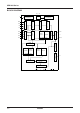
SED1220 CHIP SPECIFICATION SED1220D**/1221D**/122AD** 146 74 73 147 63 62 56 SED1220 55 165 54 1 :DUMY PAD :PAD SED122 D** ↑ Digits prepared for CGROM pattern changes * Chip size: 7.70 × 2.77 mm Pad pitch: 100 µm (Minimum) Chip thickness (for reference): 625 ± 25 µm (SED122 D*A) (SED122 D*B) * * 1) A1 pad specifications Pad size on Y side: Pad size on X side: 2) Au bump specifications Bump size on Y side: Bump size on X side: Bump height (for reference) 1) Al pad.
SED1220 SED1222D** 108 52 ......... 51 ... 109 ... y 41 ... x Top View 34 125 ... 1 ......... 11 12 27 28 SED1222D** ↑ Digits prepared for CGROM pattern changes Chip size: 7.70 × 2.77 mm Pad pitch: 124 µm (Minimum) Chip thickness (for reference): 625 ± 50 µm (SED1222D*A) 1) A1 pad specifications Pad size on Y side: Pad size on X side: 1) Al pad. pad size 90 µm × 96 µm 96 µm × 90 µm (PAD. No. 1 ~ 11, 28 ~ 32, 52 ~ 108) 175 µm ×135 µm (PAD. No.
SED1220 Name NC NC NC A0 WR CS D7 D6 D5 D4 D3 D2 D1 D0 VDD VDD VSS VSS V5 V5 V4 V4 V3 V3 V2 V2 V1 V1 V0 V0 VR VR VOUT VOUT CAP2– CAP2– CAP2+ CAP2+ CAP1– CAP1– CAP1+ CAP1+ VSS VSS VDD VDD CK VS1 P/S I/F RES NC NC NC COORDINATES X Y –3700 –1204 –3600 –3500 –3252 –3132 –3012 –2892 –2772 –2652 –2532 –2412 –2292 –2172 –2052 –1836 –1736 –1556 –1456 –1276 –1176 –996 –896 –716 –616 –436 –336 –156 –56 124 224 404 504 684 784 964 1064 1244 1344 1524 1624 1804 1904 2084 2184 2364 2464 2693 2821
SED1220 PAD No.
SED1220 Name A0 WR CS D7 D6 D5 D4 D3 D2 D1 D0 VDD VSS V5 V4 V3 V2 V1 V0 VR VOUT CAP2– CAP2+ CAP1– CAP1+ VSS VDD CK VS1 P/S I/F RES VDD (FSA) (FSB) (FSC) (FS0) (FS1) (FS2) (FS3) VDD COMSA COMS1 COM1 COM2 COM3 COM4 COM5 COM6 COM7 COM8 SEG1 SEG2 SEG3 COORDINATES X Y –3312 –1228 –3180 –3048 –2916 –2784 –2652 –2520 –2388 –2256 –2124 –1992 –1228 –1786 –1204 –1506 –1226 –946 –666 –386 –106 174 454 734 1014 1294 1574 1854 2134 2414 –1204 2692 –1228 2836 2980 3124 3268 –1228 3694 –919 3603 –796 –696 –
SED1220 PAD No.
SED1220 Name NC NC NC A0 WR CS D7 D6 D5 D4 D3 D2 D1 D0 VDD VDD VSS VSS V5 V5 V4 V4 V3 V3 V2 V2 V1 V1 V0 V0 VR VR VOUT VOUT CAP2– CAP2– CAP2+ CAP2+ CAP1– CAP1– CAP1+ CAP1+ VSS VSS VDD VDD CK VS1 P/S I/F RES NC NC NC COORDINATES X Y –3700 –1204 –3600 –3500 –3252 –3132 –3012 –2892 –2772 –2652 –2532 –2412 –2292 –2172 –2052 –1836 –1736 –1556 –1456 –1276 –1176 –996 –896 –716 –616 –436 –336 –156 –56 124 224 404 504 684 784 964 1064 1244 1344 1524 1624 1804 1904 2084 2184 2364 2464 2693 2821 2949 307
SED1220 PAD No.
SED1220 DESCRIPTION OF PINS Power Pins VS1 I/O Description Power supply Connected to logic supply. Common with MPU power terminal VCC. Power supply 0V power terminal connected to system ground. Power supply Multi-level power supply for liquid crystal drive. The voltage determined in the liquid crystal cell is resistancedivided or impedance-converted by operational amplifier, and the resultant voltage is applied. The potential is determined on the basis of VDD and the following equation must be respected.
SED1220 Pins for System Bus Connection Pin name D7 (SI) D6 (SCL) D5 ~ D0 I/O I Description 8-bit input data bus. These pins are connected to a 8-bit or 16-bit standard MPU data bus. When P/S = “Low”, the D7 and D6 pins are operated as a serial data input and a serial clock input respectively.
SED1220 Liquid Crystal Drive Circuit Signals Dynamic drive terminal (SED1220D**/1221D**/122AD**) Pin name COM1~ COM24 COMS1, CMOS2 SEG1~ SEG60 SEGS1, 2 4, 5 I/O Description Q’ty O Common signal output pin (for characters) 24 O Common signal output pin (except for characters) CMOS1, CMOS2: Common output for symbol display 2 O Segment signal output pin (for characters) 60 O Segment signal output pin (except for characters) SEGS1, SEGS2: Segment output for signal output 4 Pin name COM1~ COM16 C
SED1220 FUNCTIONAL DESCRIPTION MPU Interface Selection of interface type In the SED1220 Series, data transfer is performed through a 8-bit or 4-bit data bus or a serial data input (SI). By selecting “High” or “Low” as P/S pin polarity, a parallel data input or a serial data input can be selected as shown in Table 1.
SED1220 CS SI SCL D7 1 D6 2 D5 3 D4 4 D3 5 D2 6 D1 7 D0 8 D7 9 A0 Fig. 1 Identification of data bus signals The SED1220 series identifies data bus signals, as shown in Table 3, by combinations of A0 and WR (E). Common A0 1 0 68 series E 1 1 80 series WR 0 0 SED1220 Table 3 Function Writing to RAM and symbol register Writing to internal register (command) Chip select The SED1220 series has a chip select pin (CS). Only when CS = “Low”, MPU interfacing is enabled.
SED1220 Voltage Tripler Circuit If capacitors are connected between CAP+1 – CAP–1 and CAP2+,CAP2– and VSS VOUT, VDD– VSS potential is negatively tripled and generated at VOUT terminal. When the voltage is boosted double, open CAP2+ and connect CAP2– to VOUT terminal. At this time, the oscillating circuit must be operating since the amplifying circuit utilize the signal from the oscillation output.
SED1220 ● Voltage Regulation Circuit Using Electronic Volume Function When using the electronic volume function, you need to turn the voltage regulation circuit on using the supply control command. The electronic volume function allows to control the liquid crystal drive voltage V5 with the commands and thus to adjust density of the liquid crystal display. Liquid crystal drive voltage V5 can have one of 32 voltage values if 5-bit data is set to the electronic volume register.
SED1220 Liquid crystal voltage generating circuit V5 potential is resistive divided within IC to produce V1, V2, V3 and V4 potentials required for driving the liquid crystal. V1, V2, V3 and V4 potentials are then subject to impedance conversion and provided to the liquid crystal drive circuit. The liquid crystal drive voltage is fixed to 1/5 (1/4) bias. The liquid crystal power terminals V1 – V5 must be externally connected with the voltage regulating capacitor C2.
SED1220 Example 2: When using the built-in power source (VC, VF, P) = (1, 1, 0) Example 3: When using the built-in power source (VC, VF, P) = (0, 1, 0) SED1220D VSS ** VSS CAP1+ CAP1CAP2+ CAP2- CAP1+ CAP1CAP2+ CAP2VOUT VOUT External power source R3 V5 VR External power R2 source SED1220D ** VSS V5 VR R1 VDD, V0 C2 C2 C2 C2 C2 C2 V1 V2 V3 V4 V5 VS1 SED1220 C2 C2 C2 C2 C2 C2 VDD, V0 V1 V2 V3 V4 V5 VS1 Reference setting values: C1: 0.47 - 4.
SED1220 Low Power Consumption Mode Reset Circuit SED1220 is provided with standby mode and sleep mode for saving power consumption during standby period. Upon activation of the RES input, this LSI will be initialized. ● Standby Mode Switching between on and off of the standby mode is done using the power save command. In the standby mode, only static icon is displayed. 1.
SED1220 COMMAND C 0 0 1 1 • Command Overview Command type Display control instruction Power control System set Address control instruction Data input instruction Command name Cusor Home Display ON/OFF Control Power Save Power Control System set Address Set Data Write A0 WR 0 0 0 0 0 0 0 0 0 0 0 0 1 (C, B) A0 WR D7 D6 D5 D4 D3 D2 D1 D0 0 0 0 0 0 1 * * * * ∗ : Don't Care (2) Display ON/OFF Control This command performs on or off of display and cursor setting.
SED1220 (5) VF =0 1 : Voltage follower off : Voltage follower on VC =0 1 : Voltage regulation circuit off : Voltage regulation circuit on (6) RAM Address Set This command sets addresses to write data into the DD RAM, CG RAM and symbol register in the address counter. When the cursor is displayed, the cursor is displayed at the display position corresponding to the DD RAM address set by this command.
SED1220 (7) Data Write RAM Address Set A0 WR D7 D6 D5 D4 D3 D2 D1 D0 1 0 DATA 1 2 This command writes data the DD RAM, CG RAM or symbol register. This command automatically increases the address counter by +1, thus enabling continuous writing of data. Note: When executing NO instructions in One Line Completed? succession, reserve a time exceeding tCYC and execute the next YES instruction.
SED1220 Table 4 SED1220 Series Command List Command Code Function A0 WR D7 D6 D5 D4 D3 D2 D1 D0 (1) Cursor Home 0 0 0 0 0 1 * * * (2) Display ON/OFF Control 0 0 0 0 1 1 C B * D (3) Power Save 0 0 0 1 0 0 * (4) Power Control 0 0 0 1 0 1 0 VC VF P (5) System Set 0 0 0 1 1 0 N2 N1 S CG Sets the use or non-use of CG RAM and shifting direction of display line (N1, N2) and COM CG = 1 (use of CG RAM), 0 = (Does not use CG RAM), M2, N1 = 0, 0 (2 lines) 0, 1 (3 lines).
SED1220 SED1220DA* Lower 4 Bit of Code 0 1 2 3 4 5 6 7 8 9 A B C D E F 0 1 2 SED1220 3 4 5 Higher 4 Bit of Cord 6 7 8 9 A B C D E F EPSON 4–25
SED1220 SED1220DB* Lower 4 Bit of Code 0 1 2 3 4 5 6 7 0 1 2 3 4 5 Higher 4 Bit of Cord 6 7 8 9 A B C D E F 4–26 EPSON 8 9 A B C D E F
SED1220 SED1220DG* Lower 4 Bit of Code 0 1 2 3 4 5 6 7 8 9 A B C D E F 0 1 2 SED1220 3 4 5 Higher 4 Bit of Cord 6 7 8 9 A B C D E F EPSON 4–27
SED1220 Character Generator RAM (CG ROM) CGRAM contained in SED1220 enables user programming of character patterns for display signals with higher degrees of freedom. When using CGRAM, select it using the system command. Capacity of CGRAM is 160 bits and accepts registration of any 4 5 × 8 dots patterns. Following shows relationship between the CGRAM characters, CGRAM addresses and character code.
SED1220 Symbol Register SED1220 contains the symbol register which enable individual symbol setting for displaying on the screen. Capacity of the symbol register is 120 bits and is capable of displaying up to 120 symbols. Following shows relationship between the symbol register display patterns, RAM addresses and written data.
SED1220 up to 5 icons (SED1220/1221/1222) or 10 icons (SED122A). Following shows relationship between the static icons functions, static icon RAM addresses and written data. Static Icon Ram SED1220 contains the static icon RAM for displaying the static icons in addition to the dynamic icons.
SED1220 Item Symbol Standard value Unit VSS –6.0~+0.3 V Power supply voltage (2) V5, Vout –7.0~+0.3 V Power supply voltage (3) V1, V2, V3, V4 V5~+0.3 V Input voltage VIN VSS–0.3~+0.3 V Output voltage VO VSS–0.3~+0.3 V –30~+85 °C –55~+100 °C Power supply voltage (1) Operating temperature Storage temperature Topr TCP Bare chip Tstr (VCC) VDD –65~+125 SED1220 ABSOLUTE MAXIMUM RATINGS VDD (GND) VSS V5 Notes: 1. All the voltage values are based on VDD = 0 V. 2.
SED1220 DC CHARACTERISTICS VDD = 0 V, VSS = –3.6 V to –2.4 V, Ta = –30 to 85°C unless otherwise specified.
SED1220 ” display. This is applicable to the case where no access is made from the MPU and the built-in power circuit and oscillating circuit are in operation. *6: Current consumption when data is always written by fcyc. The current consumption in the access state is almost proportional to the access frequency (fcyc). When no access is made, only IDD (I) occurs. *7: tR (reset time) indicates the internal circuit reset completion time from the edge of the RES signal.
SED1220 TIMING CHARACTERISTICS (1) MPU Bus Write Timing (80 series) A0 tAC8 tAH8 CS tcyc8 tAW8 tCCL WR tCCH tDS8 tDH8 D0 to D7 Item Signal Address hold time A0, CS Address setup time CS setup time System cycle time WR Write “L” pulse width (WR) Write “H” pulse width (WR) Data setup time D0 ~ D7 Data hold time Item Signal Address hold time A0, CS Address setup time CS setup time System cycle time WR Write “L” pulse width (WR) Write “H” pulse width (WR) Data setup time D0 ~ D7 Data hold time [T
SED1220 (2) MPU Bus Write Timing (68 series) A0 tAH6 tAC6 CS tCYC6 tEWL tEWH E tDS6 D0 to D7 Item Signal Address setup time A0, CS Address hold time CS setup time System cycle time WR Enable “L” pulse width (WR) Enable “H” pulse width (WR) Data setup time D0 ~ D7 Data hold time Item Signal Address setup time A0, CS Address hold time CS setup time System cycle time WR Enable “L” pulse width (WR) Enable “H” pulse width (WR) Data setup time D0 ~ D7 Data hold time [Ta = –30 to 85°C, VSS = –3.
SED1220 (3) Serial Interface tCSS tCSH CS tSAS tSAH A0 tSCYC tSLW SCL tSHW tSDS tSDH SI Item System clock cycle SCL “H” pulse width SCL “L” pulse width Address setup time Address hold time Data setup time Data hold time CS-SCL time Signal Symbol SCL tSCYC tSHW tSLW tSAS tSAH tSDS tSDH tCSS tCSH A0 SI CS [Ta = –30 to 85°C, VSS = –3.6 V to –2.4 V] Measuring Min. Max. Unit condition Every timing is specified 1000 ns on the basis of 20% and 300 ns 80% of VSS.
SED1220 MPU INTERFACE (REFERENCE EXAMPLES) The SED1220 Series can be connected to the 80 series MPU and 68 series MPU. When an serial interface is used, the SED1220 Series can be operated by less signal lines.
SED1220 INTERFACE TO LCD CELLS (REFERENCE) 12 columns by 3 lines, 5 × 8-dot matrix segments and symbols SED 1220 LCD panel 1 . . . . . . . . . . . . . . . . . 12 static icon COMSA .. SEGSA SEGSE symbol COMS1 signal signal COMS2 COM1 2 3 4 5 6 7 8 COM9 10 11 12 13 14 15 16 COM17 18 19 20 21 22 23 24 character SEGS1 SEGS2 ..
SED1220 12 columns by 2 lines, 5 × 8-dot matrix segments and symbols SED 1221 LCD panel 1 ............... 12 static icon COMSA .. SEGSA SEGSE symbol COMS1 signal signal SED1220 COMS2 COM1 2 3 4 5 6 7 8 COM9 10 11 12 13 14 15 16 character SEGS1 SEGS2 ..
SED1220 12 columns by 2 lines, 5 × 8-dot matrix segments and symbols SED 1222 LCD panel 1 • • • • • • • • • • • • • • static icon COMSA .. SEGSA SEGSE symbol COMS1 COMS2 COM1 2 3 4 5 6 7 8 COM9 10 11 12 13 14 15 16 character ..
SED1220 12 columns by 2 lines, 5 × 8-dot matrix segments and symbols SED 122A LCD Panel 1 • • • • • • • • • • • • • • 12 Static icon COMSA • • SEGSA SEGSJ Symbol COMS1 COMS2 Signal Signal SED1220 COM1 2 3 4 5 6 7 8 COM9 10 11 12 13 14 15 16 Character SEGS1 SEGS2 • • SEG1 2 3 4 5 SEG60 SEGS4 SEGS5 EPSON 4–41
SED1220 LIQUID CRYSTAL DRIVE WAVEFORMS (B WAVEFORMS) COM 1 COM 2 COM 3 COM 4 COM 5 COM 6 COM 7 COM 8 VDD V1 V2 V3 V4 V5 COM 1 VDD V1 V2 V3 V4 V5 COM 2 COM 9 COM 10 COM 11 COM 12 COM 13 COM 14 COM 15 COM 16 SEG 1 SEG 2 SEG 3 SEG 4 SEG 5 VDD V1 V2 V3 V4 V5 COM 3 VDD V1 V2 V3 V4 V5 SEG 1 VDD V1 V2 V3 V4 V5 SEG 2 V5 V4 V3 V2 V1 VDD -V1 -V2 -V3 -V4 -V5 COMO -SEG 1 V5 V4 V3 V2 V1 VDD -V1 -V2 -V3 -V4 -V5 COMO -SEG 2 4–42 EPSON
SED1220 Instruction Setup Example (Reference Only) (1) Initial setup (2) Display mode VDD-VSS power ON End of initialization Power regulation Input of RAM address setup command Input of reset signal Input of RAM (data) write command Command status • Static display control: Off • Display on/off control: Off • Power save: Off • Power control: Off • System setup: Off • Electronic volume (0, 0, 0, 0, 0) • Static icon (0, 0, 0, 0, 0) • Others are undefined.
SED1220 (3-1) Selecting the Standby mode (3-2) Releasing the Standby mode Standby mode End of initialization Normal operation (Power Save is released and oscillator circuit is turned ON.
SED1220 Instruction Setup Example of SED1220 series (1) (2) (3) (4) (5) Initial setup display ON “EPSON” Display ON the Icon Standby Mode sequence Releasing the Standby Mode sequence .. SEGSE .. COM9 COMS2 SEGSA ............................. SEG60 SEGS4 SEGS5 COM24 ..
SED1220 (1) Initial setup (1.1) VDD–VSS Power ON (1.2) Power regulation (1.3) Input of RESET signal (1.4) Command Status • Display ON/OFF • Power save • Power control • System reset • Electronic Volume • Static display control • Others are undefined. :OFF :OFF :OFF :OFF :(0, 0, 0, 0, 0) :OFF (1.5) Waiting for 10µ sec or more (1.6) Command Input: ((*) indicates any command sequence.
SED1220 A0 WR D7 D6 D5 D4 D3 D2 D1 D0 1 0 0 0 1 0 0 0 0 0 1 0 0 0 1 0 0 0 0 0 1 0 0 0 1 0 0 0 0 0 1 0 0 0 1 0 0 0 0 0 1 0 0 0 1 0 0 0 0 0 1 0 0 0 1 0 0 0 0 0 1 0 0 0 1 0 0 0 0 0 1 0 0 0 1 0 0 0 0 0 1 0 0 0 1 0 0 0 0 0 1 0 0 0 1 0 0 0 0 0 1 0 0 0 1 0 0 0 0 0 1 0 0 0 1 0 0 0 0 0 1 0 0 0 1 0 0 0 0 0 SED1220 • Data writing: All data→20H (for 1 Line) • RAM address setup:
SED1220 • Data writing: All data →20H (for 3 Line) A0 WR D7 D6 D5 D4 D3 D2 D1 D0 1 0 0 0 1 0 0 0 0 0 1 0 0 0 1 0 0 0 0 0 1 0 0 0 1 0 0 0 0 0 1 0 0 0 1 0 0 0 0 0 1 0 0 0 1 0 0 0 0 0 1 0 0 0 1 0 0 0 0 0 1 0 0 0 1 0 0 0 0 0 1 0 0 0 1 0 0 0 0 0 1 0 0 0 1 0 0 0 0 0 1 0 0 0 1 0 0 0 0 0 1 0 0 0 1 0 0 0 0 0 1 0 0 0 1 0 0 0 0 0 1 0 0 0 1 0 0 0 0 0 • End of Initialization (2) Dis
SED1220 (3) Display ON The Icon: Valid in Standby mode only (3.1) Display ON/OFF command: D→OFF A0 WR D7 D6 D5 D4 D3 D2 D1 D0 0 0 0 0 1 1 0 0 0 0 (3.2) Static display control command: 1 ~ 2Hz Blink A0 WR D7 D6 D5 D4 D3 D2 D1 D0 0 0 1 0 1 0 0 0 0 0 1 0 0 0 0 1 0 0 0 0 0 0 1 0 1 0 0 0 0 1 1 0 0 0 0 1 0 0 0 0 A0 WR D7 D6 D5 D4 D3 D2 D1 D0 0 0 0 1 0 0 0/1 0/1 1 1 SED1220 (3.3) Power save command: PS→ON, 0→ON (3.
SED1220 Option List SED1220 provides the optional functions as described in the following. Being adaptable to the customer’s optional demand, contact the Business Department of our company when installed. o Our product name corresponding to a customer’s option is defined as shown below: (Example) SED1220D XB Shipping form: A (AL pad product) or B (metal bump product) 4. Power Supply to Booster Circuit SED1220 integrates a booster circuit.
SED1225 Series LCD Controller/Drivers Technical Manual
Contents OUTLINE ............................................................................................................................................................. 5–1 FEATURES .......................................................................................................................................................... 5–1 BLOCK DIAGRAM ...............................................................................................................................................
OUTLINE The SED1225 dot-matrix LCD Controller Driver receives 4-bit, 8-bit, or serial data from the microprocessor and displays up to 36 characters, four user-defined characters, and up to 120 symbols. Up to 256 types of built-in character generator ROMs are provided. Each character font has a 5×8-dot structure. Also, the user-defined character RAM contains four 5×8-dot characters. In addition, a symbolic register can be used for flexible symbol display.
SED1225 Series BLOCK DIAGRAM D0 OSC D1 D4 D5 Address Counter D6(SCL) DDRAM Symbol Register Refresh Address Counter D7(SI) Timing Generator D3 XCK Input Buffer D2 VS1 CGROM CGRAM OCA LCD Driver IF XCS XWR(E) PS C86 MPU Interface RES Command Decoder Cursor Control OCB OCC OCD OCE VREG1 VREG2 A0 V1 V3 LED Driver XLE1 XLE2 5–2 Static Icon Driver COMSA SEGSA to J V4 Segment Driver SEG1 to 60 SEGS1,2,4,5 EPSON COM Driver COM1 to 24 COMS1,2 V5
SED1225 Series PIN ASSIGNMENT 154 73 .. .................... 155 72 (0,0) ............. ............. Y X Top View 171 59 .................................... 1 58 : Dummy PAD : PAD SED1225 Series SED1225D✽✽ ↑ CGROM pattern version number Chip size: 7.85 × 1.97 mm Pad pitch: 90 µm (min) Chip thickness (Reference): 625 µm Au bump specifications Bump size: Pad Nos. 59 to 72, and 155 to 171: 78 µm × 59 µm Pad Nos. 1 to 58, and 73 to 154: 59 µm × 78 µm Bump height (Reference): 22.
SED1225 Series Pad coordinates (1/2) No.
SED1225 Series Pad coordinates (2/2) 87 88 89 90 91 92 93 94 95 96 97 98 99 100 101 102 103 104 105 106 107 108 109 110 111 112 113 114 115 116 117 118 119 120 121 122 123 124 125 126 127 128 129 PAD Name SEG11 SEG12 SEG13 SEG14 SEG15 SEG16 SEG17 SEG18 SEG19 SEG20 SEG21 SEG22 SEG23 SEG24 SEG25 SEG26 SEG27 SEG28 SEG29 SEG30 SEG31 SEG32 SEG33 SEG34 SEG35 SEG36 SEG37 SEG38 SEG39 SEG40 SEG41 SEG42 SEG43 SEG44 SEG45 SEG46 SEG47 SEG48 SEG49 SEG50 SEG51 SEG52 SEG53 Coordinate X Y 2333 2243 2153 2064 1974 1884 1
SED1225 Series PIN DESCRIPTION Power Supply Pins Pin Name I/O Description No. of Pins VDD Power supply Connects to the logic power supply. This is common to the Vcc power pin of the MPU. 1 VSS Power supply 0V power pin connected to system ground (GND) 2 Multi-level LCD drive power supplies. A capacitor is required for external Power supply stabilization. 4 V1, V3 V4, V5 VS1 O Output pin of oscillator (OSC) power voltage. A capacitor is required for stabilization.
SED1225 Series System Bus Connector Pins Pin Name I/O Descrition No. of Pins An 8-bit input data bus to be connected to the standard 8- or 16-bit MPU data bus. Pins D7 and D6 function as the serial data and clock inputs respectively if PS is logical low.
SED1225 Series LCD Driver Signals Dynamic drive pins Pin I/O Name COM1 to O COM24 COMS1, O COMS2 SEG1 to O SEG60 SEGS1, 2 O 4, 5 Description No.
SED1225 Series FUNCTION DESCRIPTION The SED1225 can transfer data via the 4- or 8-bit data bus or via the serial data input (SI). The parallel or serial data input can be selected by setting the PS pin to high or low (see Table 1). MPU Interfaces Interface type selection Table 1 PS H L Type XCS Parallel input XCS Serial input XCS A0 A0 A0 XWR XWR H, L SI – SI SCL D0 to D7 – D0 to D7 SCL – The SED1225 has the C86 pin for MPU selection.
SED1225 Series XCS SI D7 SCL 1 D6 2 D5 D4 3 D3 4 5 D2 D1 6 7 A0 D0 8 D7 1 A0 Figure 1 Data bus signal identification The SED1225 identifies the data bus based on a combination of A0, AWR and E signals as defined on Table 3. Table 3 Common 68 Series 80 Series A0 E XWR 1 1 0 0 1 0 Function Writes in the RAM and symbol register. Writes (commands) in the internal register. Chip Select The SED1225 has an Chip Select pin (XCS) to allow an MPU interface input only if XCS=low.
Voltage regulator Power Save mode • Voltage regulator using the electronic control function Use the electronic control function and set the voltages appropriate to the LCD panel driving. When a 5-bit data is set in the electronic control register, one of 32-state voltages can be set for LCD driving. Before using the electronic control function, turn ON the power circuit by issuing the power control command. The following explains how to calculate the voltages using the electronic control function.
SED1225 Series Reset Circuit When the RES input is made active, this LSI is initialized.
SED1225 Series COMMAND Table 4 lists the supported commands. The SED1225 identifies a data bus by a combination of A0, XWR and E signals. It features high-speed processing as the commands are analyzed and executed in the internal timing only.
SED1225 Series The character on the 3rd line will be displayed in double size on the second and third lines by setting DC=1. (2) N=1 (1/18 duty) DC=0 DC=1 (5) System Reset The System Reset command sets the display direction, the display line, and the use or no use of CGRAM. This command must first be executed after the power-on or reset. A0 XWR D7 D0 COM1– ... 1st line 0 0 0 1 1 ...
SED1225 Series (4) Horizontal vertical flipping SEG60 ... SEG1 (6) RAM Address Setup The RAM Address Setup command sets an address into the Address counter to write data into DDRAM, CGRAM and Symbol register. When the cursor display is ON, the cursor is located at a position corresponding to the DDRAM address set by this command. COM1 ..... A0 XWR D7 COM16 (N=1) COM24 (N=0) 0 0 D0 1 ADDRESS ✽ : Don’t Care 1 The 00H to 7FH address length can be set.
5–16 0 0 1 0 0 (5) System Reset (6) RAM Address Setup (7) RAM Write (8) NOP (9) Test Mode 0 (3) Power Save 0 0 (2) Display On/Off Control (4) Power Control 0 EPSON 0 0 0 0 0 0 0 0 0 0 0 1 0 0 0 0 0 A0 XWR D7 (1) Cursor Home Command Table 4 SED1225 command list 0 0 1 1 1 0 0 D6 0 0 1 0 0 1 0 N S2 0 ✽ ✽ 0 B ✽ ✽ C D2 D3 0 0 0 ✽ 0 ✽ DATA ADDRESS 0 1 0 1 1 D4 Code D5 ✽ 0 S1 0 0 DC ✽ D1 ✽ 0 CG P PS D ✽ D0 This is an IC chip
SED1225 Series BUILT-IN MEMORIES Character Generator ROM (CGROM) The SED1225’s CGROM is a mask ROM and it can be used as a custom CGROM. Consult to our sales agency for details. The CGROM versions are identified as follows: Example: SED1225D0B ↑ CGROM pattern ID SED1225 Series The SED1225 contains up to 126 types of CGROMs. Each character has a 5×8-dot structure. Tables 5 to 8 defines the SED1225D✽✽ character codes.
SED1225 Series Table 5 SED1225DAB Lower 4 Bit of Code 0 1 2 3 4 5 6 7 0 1 2 3 4 5 Higher 4 Bit of Cord 6 7 8 9 A B C D E F 5–18 EPSON 8 9 A B C D E F
SED1225 Series Table 6 SED1225DBB Lower 4 Bit of Code 0 1 2 3 4 5 6 7 8 9 A B C D E F 0 1 2 3 4 SED1225 Series 5 Higher 4 Bit of Cord 6 7 8 9 A B C D E F EPSON 5–19
SED1225 Series Table 7 SED1225DGB Lower 4 Bit of Code 0 1 2 3 4 5 6 7 0 1 2 3 4 5 Higher 4 Bit of Cord 6 7 8 9 A B C D E F 5–20 EPSON 8 9 A B C D E F
SED1225 Series Character Generator RAM (CGRAM) store up to four 5×8-dot character patterns. The following provides the relationship between CGRAM character patterns and CGRAM addresses and character codes.
SED1225 Series Symbol Register The SED1225 has a built-in Symbol register to allow separate symbol setup on the display panel. The Symbol register has the 120-bit storage capacity, and it can display 120 symbols. Also, the SED1225 contains a Blink register for every 5-dot blinking. 13 The following provides the relationship between the Symbol register display patterns, RAM addresses and write data. 12 1 13 1 ..... 5 56 ..... 60 61 ..... 65 116 ..... 120 2 5 .....
SED1225 Series Static Icon RAM The SED1225 has a built-in Static Icon RAM to display a static icon separately from the dynamic icon. The Static Icon RAM has the 20-bit storage capacity, and it can display 10 icons. The following provides the relationship between the static icon functions and the static icon, RAM address and write data.
SED1225 Series Electronic Control RAM (Register) The SED1225 has the electronic control functions to control LCD drive voltages and to adjust the LCD display density. One of 32-state LCD voltages can be selected when the 5-bit data is written in the Electronic Control RAM. The following provides the relationship between the RAM address and write data by electronic control setup.
SED1225 Series MAXIMUM ABSOLUTE RATINGS Item Power voltage (1) Power voltage (2) Power voltage (3) Input voltage Output voltage Operating temperature TCP Storage temperature Bare chip Symbol VSS V5 V1, V2, V3, V4 VIN VO Topr Tstr (VCC) VDD Rating –0.6 to +0.3 –7.0 to +0.3 V5 to +0.3 VSS–0.3 to +0.3 VSS–0.3 to +0.3 –30 to +85 –55 to +100 –65 to +125 Unit V V V V V °C °C VDD (GND) VSS Notes: 1. All voltages are referenced to VDD=0 V. 2.
SED1225 Series DC CHARACTERISTICS (VSS = –3.6 to –1.7 V, Ta = –30 to +85°C unless otherwise noted.) Item Power voltage (1) Power voltage (2) Symbol Operable Data hold voltage Conditions 1/4 bias VSS 1/5 bias Min. Typ. Max. –3.6 –3.0 –1.7 –3.6 –3.0 –2.7 –3.6 –1.5 Unit Pin V VSS Operable V5 –6.0 –3.0 V V5 Operable V1, V2 0.5 × V5 VDD V V1, V2 Operable V3, V4 V5 0.5 × V5 V V3, V4 "Hi" input voltage VIHC 0.2 × VSS VDD V *2 "Lo" input voltage VILC VSS 0.
SED1225 Series *1 Although the wide operating character range is guaranteed, a quick and excessive voltage variation may not be guaranteed during access by the MPU. The low-voltage data hold characteristics are valid during Sleep mode. No access by the MPU is allowed during this time. *2 D0 to D5, D6 (SCL), D7 (SI), A0, RES, XCS, XWR (E), PS, IF, C86 *3 The resistance if a 0.1-volt voltage is supplied between the SEGn, SEGSn, COMn or COMSn output pin and each power pin (V1, V2, V3 or V4).
SED1225 Series SIGNAL TIMING CHARACTERISTICS (1) MPU bus write timing (80 series) A0 tAC8 tAH8 XCS tCYC8 tAW8 tCCL XWR tCCH tDS8 tDH8 D0 to D7 (Ta = –30 to +85°C, VSS = –3.6V to –1.7V) Item Address setup time Address hold time XCS setup time Signal Symbol A0 XCS System cycle time Write "Lo" pulse width (XWR) XWR Write "Hi" pulse width (XWR) Data setup time Data hold time D0 to D7 Conditions Min. tAW8 tAH8 tAC8 tCYC8 tCCL tCCH tDS8 tDH8 All timing must be based on 20% and 80% of VSS.
SED1225 Series (2) MPU bus write timing (68 series) A0 tAH6 tAC6 XCS tCYC6 tEWH tEWL E tDS6 tDH6 tAW6 D0 to D7 Address setup time Address hold time XCS setup time Signal Symbol A0 XCS System cycle time Enable "Lo" pulse width (XWR) XWR Enable "Hi" pulse width (XWR) Data setup time Data hold time D0 to D7 Conditions Min. tAW6 tAH6 tAC6 tCYC6 tEWL tEWH tDS6 tDH6 All timing must be based on 20% and 80% of VSS. Symbol Conditions Max.
SED1225 Series (3) Serial interface tCSS tCSH XCS tSAS tSAH A0 tSCYC tSLW SCL tSHW tSDS tSDH SI (Ta = –30 to +85°C, VSS = –3.6V to –1.7V) Item System clock cycle SCL "Hi" pulse width SCL "Lo" pulse width Signal Symbol SCL Address setup time Address hold time A0 Data setup time Data hold time SI CS-to-SCL time XCS Conditions Min. tSCYC tSHW tSLW tSAS tSAH tSDS tSDH tCSS tCSH All timing must be based on 20% and 80% of VSS. Symbol Conditions Max.
SED1225 Series MPU INTERFACES (REFERENCE) The SED1225 can be connected to the 80-series or 68series MPU. Also, it can operate with a less number of signal lines via the serial interface. If the MPU buses and ports are set to high impedance for a certain time due to RESET, the RESET signal must be entered in the SED1225 after the SED1225’s inputs have been determined.
SED1225 Series LCD CELL INTERFACE 12 columns by 3 lines, 5×8 dots + Symbols SED 1225 LCD panel 1 ................. 12 columns Static Icon COMSA .. SEGSA SEGSJ Symbols Symbols COMS1 Signals Signals COMS2 COM1 2 3 4 5 6 7 8 COM9 10 11 12 13 14 15 16 COM17 18 19 20 21 22 23 24 Character SEGS1 SEGS2 ...
SED1225 Series 12 columns by 2 lines (N=1), 5×8 dots + Symbols SED 1225 LCD panel 1 • • • • • • • • • • • • • 12 columns Static icon COMSA SEGSA .. SEGSJ Symbol COMS1 Signal Signal COMS2 SED1225 Series COM1 2 3 4 5 6 7 8 COM9 10 11 12 13 14 15 16 COM17 18 19 20 21 22 23 24 Character SEGS1 SEGS2 SEG1 2 3 4 5 ...
SED1225 Series LCD DRIVE WAVEFORMS (B WAVEFORMS) COM 1 COM 2 COM 3 COM 4 COM 5 COM 6 COM 7 COM 8 VDD V1 V2 V3 V4 V5 COM 1 VDD V1 V2 V3 V4 V5 COM 2 COM 9 COM 10 COM 11 COM 12 COM 13 COM 14 COM 15 COM 16 SEG 1 SEG 2 SEG 3 SEG 4 SEG 5 VDD V1 V2 V3 V4 V5 COM 3 VDD V1 V2 V3 V4 V5 SEG 1 VDD V1 V2 V3 V4 V5 SEG 2 V5 V4 V3 V2 V1 VDD –V1 –V2 –V3 –V4 –V5 COM1 - SEG 1 V5 V4 V3 V2 V1 VDD –V1 –V2 –V3 –V4 –V5 COM1 - SEG 2 5–34 EPSON
SED1225 Series EXAMPLE OF INSTRUCTION SETUP (REFERENCE) Initialization VDD-VSS power on Power stable Reset input Command status - Static display control - Display on/off control - Power save - Power supply control - System setup - Electronic volume - Static icon Others are undefined. - off - off - off - off - 3-digit display, CGRAM unused. normal display - (0, 0, 0, 0, 0) - (0, 0, 0, 0, 0) Command input: asterisked items (*) are in no particular order.
SED1225 Series Display Mode End of initialization RAM address set input RAM (data) write input Display the written contents. Standby Mode (1) Setting the standby mode End of initialization Normal operation - Power save is cleared and oscillating circuit turns on. <1> Display on/off control command input - D off (display) <2> Power save command input - PS on (power save) O on (oscillation) <3> Power supply control command input - P off Starts the standby mode. Displays only the static icon.
SED1225 Series Sleep Mode (1) Setting the Sleep mode. End of initialization Normal operation (Power save is cleared and oscillating circuit turns on.) <1> Display on/off control command input - D off (display) <2> Power save icon control - Address 20H, 22H Data (0, 0, 0, 0, 0) - Address 21H, 23H Data (0, 0, 0, 0, 0) <3> Power save command input - PS on (power save) O off (oscillating) <4> Power supply control command input - P off (See Note 3) (See Note 3) Starts the sleep mode.
SED1225 Series OPTION LIST The SED 1225 has the following options. Options are available exclusively for users. Please contact our Sales Department for information. • The following shows how to define the name of the product compatible with options: Example: SED1225D*B ↑ Option compatibility column Specification of character generator ROM (CGROM) The SED1225 incorporates a characters generator ROM consisting of up to 256 types of characters, with each character size featuring 5 × 7 (8) dots.
SED1225 Series CAUTIONS For the use of the semi-conductor, take note of the following: “Handling cautions for light” According to the principle of the solar battery the semiconductor characteristics are changed when exposed to light. So misoperation may occur if this IC is exposed to light. For the single IC unit, measures against light are not yet completely taken.
SED1230 Series LCD Controller/Drivers Technical Manual
Contents OVERVIEW ......................................................................................................................................................... 6–1 FEATURES .......................................................................................................................................................... 6–1 BLOCK DIAGRAM ..............................................................................................................................................
OVERVIEW The SED1230 Series is a dot matrix LCD controller driver for character display, and can display a maximum of 48 characters, 4 user-defined characters, and a maximum of 64 symbols by means of 4-bit, 8-bit or serial data sent from a microcomputer. A built-in character generator ROM is prepared for 256 character types, and each character font consists of 5 × 7 dots. A user-defined character RAM for four characters of 5 × 7 dots are incorporated, and a symbol register is also incorporated.
6–2 EPSON A0 SEG1~60 SEGS1~6 SEG driving circuit COM1~28 COMS1~3 COM driving circuit Refresh address counter P/S Command decoder Address counter WR (E) Input buffer CS CG ROM Cursor control V1 V2 Oscillator RES IF RAM DD RAM CG RAM D7 (SI) D6 (SCL) D5 D4 D3 D2 D1 D0 Power circuit V3 V4 V5 VOUT VR CAP2– CAP2+ CAP1– CAP1+ VS1 SED1230 Series BLOCK DIAGRAM Timing generating circuit MPU interface
SED1230 Series SED1230 SERIES, CHIP SPECIFICATION 173 86 174 85 (0,0) 193 69 1 58 SED1230D** 1/30 duty 12 columns + 1 signal column 1/23 duty 12 columns + 1 signal column SED1231D** SED1232D** 1/16 duty 12 columns + 1 signal column 1/16 duty 16 columns SED1233D** ↑ #1 Column for CG ROM pattern change 10.23 × 3.11 mm 110 µm (Min.
SED1230 Series Unit: µm PAD No.
PAD No.
SED1230 Series Unit: µm PAD No.
PAD No.
SED1230 Series Unit: µm PAD No.
PAD No.
SED1230 Series Unit: µm PAD No.
PAD No.
SED1230 Series DESCRIPTION OF PINS Power Pins Pin name VDD VSS V0, V1 V2, V3 V4, V5 VS1 I/O Description Power supply Logic + power pin. Also used as MPU power pin VCC. Power supply Logic – power pin. Connected to the system GND. Power supply Multi-level power supply for liquid crystal drive. The voltage determined in the liquid crystal cell is resistancedivided or impedance-converted by operational amplifier, and the resultant voltage is applied.
SED1230 Series Pins for System Bus Connection I/O I Description 8-bit input data bus. These pins are connected to a 8-bit or 16-bit standard MPU data bus. When P/S = “Low”, the D7 and D6 pins are operated as a serial data input and a serial clock input respectively. P/S “Low” “High” A0 I RES I CS I WR I (E) P/S I I D6 SCL D6 D5 ~ D0 — D5 ~ D0 CS CS CS A0 A0 A0 Usually, this pin connects the least significant bit of the MPU address bus and identifies a data command.
SED1230 Series Liquid Crystal Drive Circuit Signals SED1230, SED1231, SED1232 Pin name COM1~ COM28 I/O Description Q’ty O Common signal output pin (for characters) 28 COMS1~ CMOS3 O Common signal output pin (except for characters) CMOS1: Common output for static drive. In the standby mode only, a VSS amplitude is output.
SED1230 Series FUNCTIONAL DESCRIPTION MPU Interface Selection of interface type In the SED1230 Series, data transfer is performed through a 8-bit or 4-bit data bus or a serial data input (SI). By selecting “High” or “Low” as P/S pin polarity, a parallel data input or a serial data input can be selected as shown in Table 1.
SED1230 Series CS S1 SCL D7 1 D6 2 D5 3 D4 4 D3 5 D2 6 D1 7 D0 8 D7 9 A0 Fig. 1 Identification of data bus signals The SED1230 series identifies data bus signals, as shown in Table 3, by combinations of A0 and WR (E). Table 3 Common A0 1 0 68 series E 1 1 80 series WR 0 0 Function Writing to RAM and symbol register Writing to internal register (command) Chip select The SED1230 series has a chip select pin (CS). Only when CS = “Low”, MPU interfacing is enabled.
SED1230 Series Triple boosting circuit When a capacitor is connected between CAP1+ and CAP1-, between CAP2+ and CAP2-, and between VSS pin and VOUT pin respectively, the potential between the VDD pin and VSS pin is boosted triple and output to the V OUT pin. In case of double boosting, remove the capacitor between CAP2+ and CAP2- in connection for triple boosting operation and strap between CAP2- and VOUT pin. Then, a double boosted output can be obtained from the VOUT pin (CAP2-).
SED1230 Series ● Voltage Regulation Circuit Using Electronic Contrast Control Register The contrast control register controls the liquid crystal driving voltage (V5). This is accomplished by an electronic volume control register set command that adjusts the contrast of the liquid crystal display (see section 122). The commands provide 4-bits of voltage level data to the electronic volume control register. This provides for the selection of 16 different voltage levels for the liquid crystal driving voltage.
SED1230 Series Liquid crystal voltage generating circuit The V5 potential is resistance-divided inside the IC so that V1, V2, V3 and V4 potentials are generated for liquid crystal drive. Furthermore, the V1, V2, V3 and V4 are impedanceconverted by voltage follower and the then supplied to the liquid crystal drive circuit. The liquid crystal drive voltage is fixed to 1/5 bias.
SED1230 Series ecuted, the sleep mode is set. This mode permits reducing current consumption nearly to the static current value. 1. Liquid crystal display output COM1 ~ COM28, COMS2, COMS3 : VDD level SEG1 ~ SEG60, SEGS2 ~ SEGS6 : VDD level COMS1 ~ SEGS1 : VDD level 2. DD RAM, CG RAM and symbol register Written contents do not change and are stored regardless of whether the sleep mode is turned on or off. 3. In the operation mode, the status precedent to execution of the sleep mode is held.
SED1230 Series COMMANDS (3) Table 4 shows a command list. In the SED1230 Series, each data bus signal is identified by a combination of A0 and WR (E). Command interpretation and execution are performed by only internal timing. This permits high-speed processing. Note: Control the symbols that are driven by COMS1 and SEGS1, by the Static Display Control command.
SED1230 Series (4) Power Save This command is used to control the oscillating circuit and set and reset the standby mode or sleep mode. (7) Electronic Volume Register Set This command controls the liquid crystal driving voltage V5 output from the voltage regulating circuit of the built-in liquid crystal power supply, thereby adjusting the gradation of liquid crystal display. When data is set in the 4-bit register, the liquid crystal driving voltage can take one of 16 voltage states.
SED1230 Series RAM Map (SED1230, SED1231, SED1232) 1 2 3 4 5 C G R A M (0 0 H) C G R A M (0 2 H) 6 7 8 – – Unused DDRAM line 1 DDRAM line 2 DDRAM line 3 DDRAM line 4 Symbol register 9 A B C D C G R A M (0 1 H) C G R A M (0 3 H) For signals E F – – Unused " " " " ------------- 0 00H 10H 20H 30H 40H 50H 60H 70H – : Unused For signals : Output from SEGS2 to SEGS6.
SED1230 Series Table 4 SED1230 Series Command List Command Code A0 WR D7 D6 D5 D4 D3 D2 D1 D0 (1) Cursor Home 0 0 0 0 0 1 * * (2) Static Display Control 0 0 0 0 1 0 * * SD1 Sets the display mode of static display symbol SD0 SD1, SD0 = 0, 0 (display OFF), 0, 1 (1 - 2 Hz blink), 1, 0 ( 3 4 Hz blink), 1, 1 (all display ON) (3) Display ON/OFF Control 0 0 0 0 1 1 C B DC D (4) Power Save 0 0 0 1 0 0 * (5) Power Control 0 0 0 1 0 1 0 VC VF P (6) System Set 0 0 0 1 1
SED1230 Series CHARACTER GENERATOR Character Generator ROM (CG ROM) The CG ROM of the SED1230 Series is a mask ROM and compatible with the user-dedicated CG ROM. Please ask us for further information of it. The SED1230 Series is provided with a character generator ROM consisting of a up to 256-type characters. Each character size is 5 × 7 dots.
SED1230 Series SED123* DA* Table 5 Lower 4 Bit of Code 0 1 2 3 4 5 6 7 8 0 1 2 3 4 5 Higher 4 Bit of Cord 6 7 8 9 A B C D E F 6–26 EPSON 9 A B C D E F
SED1230 Series SED123* DB* Lower 4 Bit of Code 0 1 2 3 4 5 6 7 8 9 A B C D E F 0 1 2 3 4 5 SED1230 Series Higher 4 Bit of Cord 6 7 8 9 A B C D E F EPSON 6–27
SED1230 Series SED123* DG* Lower 4 Bit of Code 0 1 2 3 4 5 6 7 0 1 2 3 4 5 Higher 4 Bit of Cord 6 7 8 9 A B C D E F 6–28 EPSON 8 9 A B C D E F
SED1230 Series Character Generator RAM (CG RAM) The SED1230 Series is provided with a CG RAM that permits user-programming character patterns so that they can be displayed with a high degree of freedom for signal display. Before using the CG RAM, select the use of CG RAM by the System Set command. The capacity of the CG RAM is 140 bits and arbitrary patterns of 4 types consisting of 5 × 7 dots can be registered. The relationship among CG RAM patterns, CG RAM addresses, and character codes is shown below.
SED1230 Series Symbol Register The SED1230 Series is provided with a symbol register that permits displaying each symbol so that symbol display may be performed on the screen. The capacity of the symbol register is 64 bits. In case of 12 digits, 48 symbols can be displayed. In case of 16 digits, 64 symbols can be displayed. The relationship among symbol register display patterns, RAM addresses and write data is shown below.
SED1230 Series SED1233 1 2 Symbol 1 2 E 3 4 31 32 27 28 63 64 COMS2 COMS3 25 26 SEG2 SEG4 SEG7 SEG9 RAM address 70H~7FH Notes 0 1 : E F SEG77 SEG79 Symbol Bits D7 D6 D5 D4 D3 D2 * * * 33 1 34 * * * 35 3 36 : 61 29 62 * * * 63 31 64 * * * D1 D0 Bit 2 * 1: Display 4 * 0: Not display 30 32 SED1230 Series (2) * * 1: If the symbol segment size is 1.5 times or more greater than the other dots, it is recommended to be divided into COMS2 and COMS3 and driven separately.
SED1230 Series ABSOLUTE MAXIMUM RATINGS Item Symbol Standard value Unit VSS –6.0~+0.3 V Power supply voltage (2) V5 –12.0~+0.3 V Power supply voltage (3) V1, V2, V3, V4 V5~+0.3 V Input voltage VIN VSS–0.3~+0.3 V Output voltage VO VSS–0.3~+0.3 V –30~+85 °C –55~+100 °C Power supply voltage (1) Operating temperature Storage temperature Topr TCP Bare chip Tstr (VCC) VDD –65~+125 VDD (GND) VSS V5 Notes: 1. All the voltage values are based on VDD = 0 V. 2.
SED1230 Series DC CHARACTERISTICS VDD = 0 V, VSS = –3.6 V to –2.4 V, Ta = –30 to 85°C unless otherwise specified. Reset time Reset pulse width Reset start time Built-in power supply Input voltage Booster output voltage Voltage follower operating voltage Reference voltage (standard) Reference voltage (option 1) Reference voltage (option 2) tR tRW tRES VSS VOUT –3.6 –7.2 –10.8 –11.
SED1230 Series *5: Character “ ” display. This is applicable to the case where no access is made from the MPU and the built-in power circuit and oscillating circuit are in operation. *11: The fOSC frequency of the oscillator circuit for internal circuit drive may differ from the fBST boosting clock on some models. The following provides the relationship between the fOSC frequency, fBST boosting clock, and fFR frame frequency. fOSC = (No. of digits) × (1/Duty) × fFR fBST = (1/2) × (1/No.
SED1230 Series TIMING CHARACTERISTICS (1) System Bus Write Characteristic I (80 series MPU) tAH8 A0, CS tAW8 tCYC8 tCC WR tDS8 tDH8 Item Address hold time Address setup time System cycle time Control pulse width (WR) Data setup time Data hold time [VSS = –3.6 V to –2.4 V, Ta = –30 to 85°C unless otherwise specified] Measuring Signal Symbol Min. Max. Unit condition A0, CS t AH8 30 ns t AW8 60 ns WR t CYC8 VSS = –3.0 500 ns –2.7 550 –2.4 650 t CC VSS = –3.0 100 ns –2.7 120 –2.
SED1230 Series (2) System Bus Write Characteristic II (68 series MPU) tCYC6 E tAW6 tEW tAH6 A0, CS tDS6 tDH6 D0 to D7 Item System cycle time Address setup time Address hold time Data setup time Data hold time Enable pulse width [VSS = –3.6 V to –2.4 V, Ta = –30 to 85°C unless otherwise specified] Measuring Signal Symbol Min. Max. Unit condition A0, CS t CYC6 VSS = –3.0 500 ns –2.7 550 –2.4 650 t AW6 60 t AH6 30 ns D0 ~ D7 t DS6 100 ns t DH6 50 ns E t EW VSS = –3.0 100 ns –2.7 120 –2.
SED1230 Series (3) Serial Interface tCSS tCSH CS tSAS tSAH A0 tSCYC tSLW SCL tSHW tSDH SED1230 Series tSDS SI Item System clock cycle SCL “H” pulse width SCL “L” pulse width Address setup time Address hold time Data setup time Data hold time CS-SCL time Signal Symbol SCL tSCYC A0 SI CS tSHW tSLW tSAS tSAH tSDS tSDH tCSS tCSH [VSS = –3.6 V to –2.4 V, Ta = –30 to 85°C] Measuring Min. Max. Unit condition VSS = –3.0 700 ns –2.7 800 ns –2.4 1000 ns 300 ns 300 ns 50 ns VSS = –3.
SED1230 Series MPU INTERFACE (REFERENCE EXAMPLES) The SED1230 Series can be connected to the 80 series MPU and 68 series MPU. When an serial interface is used, the SED1230 Series can be operated by less signal lines.
SED1230 Series INTERFACE TO LCD CELLS (REFERENCE) 12 columns by 2 lines, 5 × 7-dot matrix segments and symbols 1 • • • • • • • • • • • • • • 12 SED1232 COMS1 SEGS1 COMS2 COMS3 COM1 2 3 4 5 6 7 SED1230 Series COM8 9 10 11 12 13 14 SEGS2 3 4 SEG1 2 3 4 5 : : SEG60 SEGS4 5 6 ■ System Setup N2 0 N1 0 EPSON 6–39
SED1230 Series LIQUID CRYSTAL DRIVE WAVEFORMS (B WAVEFORMS) COM 1 COM 2 COM 3 COM 4 COM 5 COM 6 COM 7 COM 8 COM 9 COM 10 COM 11 COM 12 COM 13 COM 14 VDD V1 V2 V3 V4 V5 COM 1 VDD V1 V2 V3 V4 V5 COM 2 VDD V1 V2 V3 V4 V5 COM 3 SEG 1 SEG 2 SEG 3 SEG 4 SEG 5 VDD V1 V2 V3 V4 V5 SEG 1 VDD V1 V2 V3 V4 V5 SEG 2 V5 V4 V3 V2 V1 VDD -V1 -V2 -V3 -V4 -V5 COMO -SEG 1 V5 V4 V3 V2 V1 VDD -V1 -V2 -V3 -V4 -V5 COMO -SEG 2 6–40 EPSON
SED1230 Series Instruction Setup Example (Reference Only) (1) Initial setup (2) Display mode VDD-VSS power ON End of initialization Power regulation Input of RAM address setup command Input of reset signal Input of RAM (data) write command Command status • Static display control • Display on/off control • Power save • Power control • System reset • Others are undefined.
SED1230 Series (3-1) Selecting the Standby mode (3-2) Releasing the Standby mode End of initialization Standby mode Normal operation (Power Save is released and oscillator circuit is turned ON.
SED1234/35 Series LCD Controller/Drivers Technical Manual
Contents OVERVIEW ......................................................................................................................................................... 7–1 FEATURES .......................................................................................................................................................... 7–1 BLOCK DIAGRAM ..............................................................................................................................................
SED1234/35 Series OVERVIEW The SED1234, 1235 Series is a dot matrix LCD controller driver for character display, and can display a maximum of 48 characters, 4 user-defined characters, and a maximum of 48 symbols by means of 4-bit, 8-bit or serial data sent from a microcomputer. A built-in character generator ROM is prepared for 256 character types, and each character font consists of 5 × 7 dots.
7–2 EPSON A0 Input buffer SEG1~60 SEGS2, 6 SEG driving circuit COM1~28 COMS2, 3 COM driving circuit Refresh address counter P/S Command decoder Address counter WR (E) CG ROM CS RAM Cursor control V1 V2 Oscillator RES IF D7 (SI) D6 (SCL) D5 D4 D3 D2 D1 D0 Power circuit V3 V4 V5 VOUT VR CAP2– CAP2+ CAP1– CAP1+ VS1 SED1234/35 Series BLOCK DIAGRAM Timing generating circuit MPU interface
SED1234/35 Series SED1234/35 SERIES, CHIP SPECIFICATION 109 33 · · · · · · · · · · · 110 32 ····· (0, 0) ·· Y X 22 21 127 · · · · · · 1 2 3 17 14 15 16 : NC (Make it floating.) ↑ 1/30 duty 1/16 duty SED1234/35 Series SED1234D** SED1235D** #1 Column for CG ROM pattern change Chip size: Pad pitch: Chip thickness: 1) A1 pad specification Pad size: 10.23 × 3.11 mm 126 µm (Min.
SED1234/35 Series (1/2) PAD No.
SED1234/35 Series (2/2) Name COM21 COM20 COM19 COM18 COM17 COM16 COM15 COMS3 A0 WR CS D7 D6 D5 D4 D3 D2 D1 D0 COORDINATES X Y –4933 1405 –4964 1094 966 839 712 584 457 330 202 75 –52 –180 –307 –434 –562 –689 –816 –943 –1071 SED1234/35 Series PAD No.
SED1234/35 Series (1/2) PAD No.
SED1234/35 Series (2/2) Name COM14 COM13 COM12 COM11 COM10 COM9 COM8 COMS3 A0 WR CS D7 D6 D5 D4 D3 D2 D1 D0 COORDINATES X Y –4933 1405 –4964 1094 966 839 712 584 457 330 202 75 –52 –180 –307 –434 –562 –689 –816 –943 –1071 SED1234/35 Series PAD No.
SED1234/35 Series DESCRIPTION OF PINS Power Pins Pin name VDD VSS V0, V1 V2, V3 V4, V5 VS1 I/O Description Power supply Logic + power pin. Also used as MPU power pin VCC. Power supply Logic – power pin. Connected to the system GND. Power supply Multi-level power supply for liquid crystal drive. The voltage determined in the liquid crystal cell is resistancedivided or impedance-converted by operational amplifier, and the resultant voltage is applied.
SED1234/35 Series Pins for System Bus Connection I/O I Description 8-bit input data bus. These pins are connected to a 8-bit or 16-bit standard MPU data bus. When P/S = “Low”, the D7 and D6 pins are operated as a serial data input and a serial clock input respectively. P/S “Low” “High” A0 I RES I CS I WR I (E) P/S I I D6 SCL D6 D5 ~ D0 — D5 ~ D0 CS CS CS A0 A0 A0 Usually, this pin connects the least significant bit of the MPU address bus and identifies a data command.
SED1234/35 Series Liquid Crystal Drive Circuit Signals SED1234 Pin name COM1~ COM28 COMS2, CMOS3 SEG1~ SEG60 SEGS2, SEGS6 SED1235 Pin name COM1~ COM14 COMS2, CMOS3 SEG2~ SEG60 SEGS2, SEGS6 7–10 I/O Description Q’ty O Common signal output pin (for characters) 28 O Common signal output pin (except for characters) CMOS2, CMOS3: Common output for symbol display 2 O Segment signal output pin (for characters) 60 O Segment signal output pin (except for characters) SEGS2, SEGS6: Segment output for s
SED1234/35 Series FUNCTIONAL DESCRIPTION MPU Interface Selection of interface type In the SED1234, SED1235, data transfer is performed through a 8-bit or 4-bit data bus or a serial data input (SI). By selecting “High” or “Low” as P/S pin polarity, a parallel data input or a serial data input can be selected as shown in Table 1.
SED1234/35 Series CS S1 SCL D7 1 D6 2 D5 3 D4 4 D3 5 D2 6 D1 7 D0 8 D7 9 A0 Fig. 1 Identification of data bus signals The SED1234, SED1235 series identifies data bus signals, as shown in Table 3, by combinations of A0 and WR (E). Table 3 Common A0 1 0 68 series E 1 1 80 series WR 0 0 Function Writing to RAM and symbol register Writing to internal register (command) Chip select The SED1234, SED1235 series has a chip select pin (CS). Only when CS = “Low”, MPU interfacing is enabled.
SED1234/35 Series Triple boosting circuit When a capacitor is connected between CAP1+ and CAP1-, between CAP2+ and CAP2-, and between VSS pin and VOUT pin respectively, the potential between the VDD pin and VSS pin is boosted triple and output to the V OUT pin. In case of double boosting, remove the capacitor between CAP2+ and CAP2- in connection for triple boosting operation and strap between CAP2- and VOUT pin. Then, a double boosted output can be obtained from the VOUT pin (CAP2-).
SED1234/35 Series ● Voltage Regulation Circuit Using Electronic Contrast Control Register The contrast control register controls the liquid crystal driving voltage (V5). This is accomplished by an electronic volume control register set command that adjusts the contrast of the liquid crystal display (see section 122). The commands provide 4-bits of voltage level data to the electronic volume control register.
SED1234/35 Series Liquid crystal voltage generating circuit The V5 potential is resistance-divided inside the IC so that V1, V2, V3 and V4 potentials are generated for liquid crystal drive. Furthermore, the V1, V2, V3 and V4 are impedanceconverted by voltage follower and the then supplied to the liquid crystal drive circuit. The liquid crystal drive voltage is fixed to 1/5 bias.
SED1234/35 Series Low Power Consumption Mode Reset Circuit The SED1234, SED1235 Series is provided with the standby mode and sleep mode with the object of low power consumption when the unit is in the standby state. When the RES input goes active, this LSI enters the initialization status. ● Sleep Mode After the power circuit and oscillating circuit are turned off by command and the power save command is executed, the sleep mode is set.
SED1234/35 Series COMMANDS B = 0 : Cursor blink OFF 1 : Cursor blink ON In the blink state, display characters in normal video and display characters in monochrome reverse video are displayed alternately. The repetition cycle of alternate display is about 1 second. Table 4 shows a command list. In the SED1230 Series, each data bus signal is identified by a combination of A0 and WR (E). Command interpretation and execution are performed by only internal timing. This permits high-speed processing.
SED1234/35 Series (4) thereby adjusting the gradation of liquid crystal display. When data is set in the 4-bit register, the liquid crystal driving voltage can take one of 16 voltage states. Power Control This command is used to control the operation of the built-in power circuit.
SED1234/35 Series (8) Data Write RAM Address Set A0 WR D7 D6 D5 D4 D3 D2 D1 D0 DATA 1 0 1 2 This command writes data into the DD RAM, CG RAM or symbol register. After this command is executed, the address counter is automatically incremented by 1. This permits writing data in succession. NO One Line Completed? YES Note: When executing instructions in succession, reserve a time exceeding tCYC and execute the next instruction.
SED1234/35 Series Table 4 SED1234/SED1235 Command List Command Code A0 WR D7 D6 D5 D4 D3 D2 D1 D0 (1) Cursor Home 0 0 0 0 0 1 (2) Display ON/OFF Control 0 0 0 0 1 1 C B DC D (3) Power Save 0 0 0 1 0 0 * (4) Power Control 0 0 0 1 0 1 0 VC VF P (5) System Set 0 0 0 1 1 0 N2 N1 * CG Sets the use or non-use of CG RAM and display lines (N2, N1).
SED1234/35 Series CHARACTER GENERATOR Character Generator ROM (CG ROM) The CG ROM of the SED1234/1235 is a mask ROM and compatible with the use-dedicated CG ROM. Please ask us for further information of it. The SED1234/1235 is provided with a character generator ROM consisting of a up to 256-type characters. Each character size is 5 × 7 dots.
SED1234/35 Series Table 5 SED123 DA* * Lower 4 Bit of Code 0 1 2 3 4 5 6 7 0 1 2 3 4 5 Higher 4 Bit of Cord 6 7 8 9 A B C D E F 7–22 EPSON 8 9 A B C D E F
SED1234/35 Series SED123 DB* * Lower 4 Bit of Code 0 1 2 3 4 5 6 7 8 9 A B C D E F 0 1 2 3 4 5 7 SED1234/35 Series Higher 4 Bit of Cord 6 8 9 A B C D E F EPSON 7–23
SED1234/35 Series SED123 DG* * Lower 4 Bit of Code 0 1 2 3 4 5 6 7 8 0 1 2 3 4 5 Higher 4 Bit of Cord 6 7 8 9 A B C D E F 7–24 EPSON 9 A B C D E F
SED1234/35 Series Character Generator RAM (CG RAM) The SED1230 Series is provided with a CG RAM that permits user-programming character patterns so that they can be displayed with a high degree of freedom for signal display. Before using the CG RAM, select the use of CG RAM by the System Set command. The capacity of the CG RAM is 140 bits and arbitrary patterns of 4 types consisting of 5 × 7 dots can be registered. The relationship among CG RAM patterns, CG RAM addresses, and character codes is shown below.
SED1234/35 Series Symbol Register The SED1234, 1235 provided with a symbol register that permits displaying each symbol so that symbol display may be performed on the screen. The capacity of the symbol register is 48 bits. In case of 48 symbols can be displayed. The relationship among symbol register display patterns, RAM addresses and write data is shown below.
SED1234/35 Series ABSOLUTE MAXIMUM RATINGS Item Symbol Standard value Unit VSS –6.0~+0.3 V Power supply voltage (2) V5 –16.0~+0.3 V Power supply voltage (3) V1, V2, V3, V4 V5~+0.3 V Input voltage VIN VSS–0.3~+0.3 V Output voltage VO VSS–0.3~+0.3 V Operating temperature Topr –30~+85 °C –55~+100 °C Power supply voltage (1) Storage temperature TCP Bare chip Tstr (VCC) VDD –65~+125 VDD (GND) VSS V5 SED1234/35 Series Notes: 1. All the voltage values are based on VDD = 0 V.
SED1234/35 Series DC CHARACTERISTICS VDD = 0 V, VSS = –3.6 V to –2.4 V, Ta = –30 to 85°C unless otherwise specified. Item Symbol Condition min typ max Recommended –3.6 –3.0 –2.4 operation VSS Operable –5.5 –3.0 –2.4 Recommended –8.0 –5.0 operation V5 Operable –11.0 –4.5 Operable V1, V2 0.6×V5 VDD Operable V3, V4 VDD 0.4×V5 High-level input voltage VIHC 0.2×VSS VDD Low-level input voltage VILC VSS 0.8×VSS Input leakage current ILI VIN = VDD or VSS –1.0 1.0 µA LC driver ON resistance RON Ta=25°C V5=–7.
SED1234/35 Series *6: This is applicable to the case where the built-in power circuit is OFF and the oscillating circuit is in operation in the standby mode. *10: When operating the boosting circuit, the power supply VSS must be used within the input voltage range. *7: Current consumption when data is always written by fcyc. The current consumption in the access state is almost proportional to the access frequency (fcyc). When no access is made, only IDD (I) occurs.
SED1234/35 Series TIMING CHARACTERISTICS (1) System Bus Write Characteristic I (80 series MPU) tAH8 A0, CS tAW8 tCYC8 tCC WR tDS8 tDH8 D0 to D7 Item Address hold time Address setup time System cycle time Control pulse width (WR) Data setup time Data hold time [VSS = –3.6 V to –2.4 V, Ta = –30 to 85°C unless otherwise specified] Measuring Signal Symbol Min. Max. Unit condition A0, CS t AH8 30 ns t AW8 60 ns WR t CYC8 VSS = –3.0 500 ns –2.7 550 –2.4 650 t CC VSS = –3.0 100 ns –2.7 120 –2.
SED1234/35 Series (2) System Bus Write Characteristic II (68 series MPU) tCYC6 E tAW6 tEW tAH6 A0, CS tDS6 tDH6 Item System cycle time Address setup time Address hold time Data setup time Data hold time Enable pulse width [VSS = –3.6 V to –2.4 V, Ta = –30 to 85°C unless otherwise specified] Measuring Signal Symbol Min. Max. Unit condition A0, CS t CYC6 VSS = –3.0 500 ns –2.7 550 –2.4 650 t AW6 60 t AH6 30 ns D0 ~ D7 t DS6 100 ns t DH6 50 ns E t EW VSS = –3.0 100 ns –2.7 120 –2.
SED1234/35 Series (3) Serial Interface tCSS tCSH CS tSAS tSAH A0 tSCYC tSLW SCL tSHW tSDS tSDH SI [VSS = –3.6 V to –2.4 V, Ta = –30 to 85°C] Measuring Item Signal Symbol Min. Max. Unit condition System clock cycle SCL tSCYC VSS = –3.0 700 ns –2.7 800 ns –2.4 1000 ns SCL “H” pulse width tSHW 300 ns SCL “L” pulse width tSLW 300 ns Address setup time A0 tSAS 50 ns Address hold time tSAH VSS = –3.0 350 ns –2.7 400 ns –2.
SED1234/35 Series MPU INTERFACE (REFERENCE EXAMPLES) The SED1234, 1235 can be connected to the 80 series MPU and 68 series MPU. When an serial interface is used, the SED1234, 1235 Series can be operated by less signal lines.
SED1234/35 Series INTERFACE TO LCD CELLS (REFERENCE) 12 columns by 2 lines, 5×7-dot matrix segments and symbols • • • • 1 • • • • • • • • • • 12 SED 1235 COMS2 COMS3 COM1 2 3 4 5 6 7 COM8 9 10 11 12 13 14 SEGS2 SEG1 2 3 4 5 ·· ·· SEG60 SEGS4 ■ System Setup 7–34 N2 N1 0 0 EPSON
SED1234/35 Series LIQUID CRYSTAL DRIVE WAVEFORMS (B WAVEFORMS) COM 8 COM 9 COM 10 COM 11 COM 12 COM 13 COM 14 SEG 1 SEG 2 SEG 3 SEG 4 SEG 5 VDD V1 V2 V3 V4 V5 COM 1 VDD V1 V2 V3 V4 V5 COM 2 VDD V1 V2 V3 V4 V5 COM 3 VDD V1 V2 V3 V4 V5 SEG 1 VDD V1 V2 V3 V4 V5 SEG 2 V5 V4 V3 V2 V1 VDD -V1 -V2 -V3 -V4 -V5 COMO -SEG 1 V5 V4 V3 V2 V1 VDD -V1 -V2 -V3 -V4 -V5 COMO -SEG 2 EPSON 7–35 SED1234/35 Series COM 1 COM 2 COM 3 COM 4 COM 5 COM 6 COM 7
SED1234/35 Series Instruction Setup Example (Reference Only) (1) (2) Initial setup Display mode VDD-VSS power ON End of initialization Power regulation Input of RAM address setup command Input of reset signal Input of RAM (data) write command Command status • Static display control • Display on/off control • Power save • Power control • System reset • Others are undefined.
SED1234/35 Series (3-2) Releasing the Standby mode (3-1) Selecting the Standby mode End of initialization Standby mode Normal operation (Power Save is released and oscillator circuit is turned ON.
SED1240 Series LCD Controller/Drivers Technical Manual
Contents OVERVIEW .......................................................................................................................................................... 8-1 FEATURES ........................................................................................................................................................... 8-1 BLOCK DIAGRAM ................................................................................................................................................
OVERVIEW The SED1240 Series is a character display dot matrix LCD controller driver. This driver can display up to 64 characters and 6 user-defined characters, and up to 160 symbols according to the 4-bit, 8-bit or serial data which is sent from a microcomputer. The built-in character generator ROM is provided with up to 544 types of character fonts having a structure of 5 × 8 dots. Up to 256 types can be continuously called by register option selection.
SED1240 Series D0 D1 D2 D3 D4 D5 D6 (SCL) D7 (SI) Input buffer BLOCK DIAGRAM IR register (extended register) Address counter DDRAM symbol register Refresh address counter Vertical double-size display control circuit CGROM CGRAM Line scroll control circuit Timing generating circuit Oscillating circuit VS 1 CK CAP 1+ CAP 1– CAP2+ Command decoder CS WR (E) P/S A0 C86 Line/cursor blink control circuit MPU interface RES To each power control circuit LCD power circuit CAP2– IF VR VOUT V1 V2
SED1240 Series CHIP SPECIFICATIONS 185 101 ........................ 186 100 SED1240 Series ..... ..... D124XDXX Y Die No. X (0, 0) 210 ........................ 1 2 3 4 5 75 6 74 : DUMMY PAD : PAD SED124 ** ** ↑ ↑ Digits for CGROM pattern change Number of display lines 0: 4-line display 1: 3-line display 2: 2-line display Chip size: 8.70 × 2.80 mm Pad pitch: 90 µm (Min.
SED1240 Series SED1240*** No.
PAD COORDINATES PAD X Y No. Name [BUMP TYPE] No.
SED1240 Series SED1241*** No.
No.
SED1240 Series SED1242*** No.
No.
SED1240 Series DESCRIPTION OF PINS Power Pins Pin name I/O Description Q’ty Board potential IC board is based on VDD potential. To lock the board potential with VDD. VDD Power supply Connected to the logic power supply. This is used in common with 6 the MPU power pin VCC. VSS Power supply 0 V power pin that is connected to system GND. 4 V0, V1 Power supply Multi-level power supply for liquid crystal drive.
SED1240 Series System Bus Connecting Pins I/O I Description 8-bit input data bus which is connected to the 16-bit standard MPU data bus. Pin D7 and pin D6 function as a serial data input and a serial clock input at P/S = “L”, respectively.
SED1240 Series Liquid Crystal Drive Circuit Signals Dynamic Drive Pins [SED1240] Pin name COM1 to COM32 COMS1, COMS2 SEG1 to SEG80 I/O Description Q’ty O Common signal output pins (for characters) 32 O Common signal output pins (for others than characters) COMS1, COMS2: Symbol output command output 4 O Segment signal output pins (for characters) 80 Dynamic Drive Pins [SED1241] Pin name COM1 to COM24 COMS1, COMS2 SEG1 to SEG80 I/O Description Q’ty O Common signal output pins (for characters
SED1240 Series DESCRIPTION OF FUNCTIONS MPU Interfaces In the SED1240 series, an MPU type, interface bit length and interface method can be selected depending on pins IF, P/ S and C86. Selection of MPU In the SED1240 series, when parallel input is selected (P/S = “H”), pin C86 has an MPU selecting function. When either “H” or “L” is selected as the polarity of pin C86, the 80 series MPU or 68 series MPU can be selected as shown in Table 1.
SED1240 Series Fig. 1 shows a timing chart of the serial interface. In case of the SCL signal, extreme care should be taken about terminal reflection and external noise due to a wiring length. Accordingly, it is recommended to make an operation check. It is also recommended to periodically refresh the each command write state to prevent a malfunction from being caused by noise. CS D7 (SI) D7 D6 (SCL) D6 1 2 D5 3 D4 4 D3 5 D2 6 D1 7 D0 8 D7 1 A0 Fig.
SED1240 Series Boosting circuit The SED1240 series is provided with a boosting circuit for triple boosting and double boosting for the potential between VDD and VSS2. For triple boosting, connect a capacitor between CAP1+ and CAP1–, between CAP2+ and CAP2–, and between VDD and VOUT, and the VDD - VSS2 potential is tripleboosted to the negative side and output to the VOUT pin.
SED1240 Series Voltage regulating circuit The boosting voltage generated at VOUT is output as a liquid crystal drive voltage of V5 through the voltage regulating circuit. The SED1240 series is provided with a high-precision constant-voltage source, a 32-step electronic volume function, and a V5 voltage regulating resistor. This permits constructing a high-precision voltage regulating circuit with a small quantity of parts.
SED1240 Series [When using the V5 voltage regulating built-in resistor (Use of V5 voltage regulating built-in resistor is set by command.)] When the V5 voltage regulating built-in resistor and the electronic volume function are used, the liquid crystal supply voltage V5 can be controlled and the density of liquid crystal display can be controlled by commands only without adding any external resistor.
SED1240 Series • Voltage regulating circuit using the electronic volume function When the electronic volume function is used, the liquid crystal drive voltage V5 can be controlled by the command to adjust the density of liquid crystal display. Regarding this method, set 5-bit data in the electronic volume register, and the liquid crystal drive voltage V5 can take one of 32 states of voltage value.
SED1240 Series Liquid crystal voltage generating circuit The V5 potential is resistance-divided by the built-in resistor of the IC or external resistors Ra and Rb, generating potentials V1, V2, V3, and V4 required for liquid crystal drive. Furthermore, potentials V1, V2, V3, and V4 are impedance-converted by the voltage follower and supplied to the liquid crystal drive circuit. Regarding the liquid crystal drive voltage, the 1/5 bias or 1/4 bias can be selected by command.
SED1240 Series 2 Using only the voltage regulating circuit and the voltage follower.
SED1240 Series Low Power Consumption Mode The SED1240 series is provided with the standby mode/ sleep mode to attain low power consumption in the standby status of the unit. ● Standby mode The standby mode is turned on and off by the power save command and display off/booster circuit off command. Only static icons can be displayed. 1.
SED1240 Series pulses at least for 10 µs as described in DC Characteristics. The ordinary operation will be started in 1 µs or more after the rising edge of the RES signal. When the RES pin becomes active, each register will be cleared and set to the above setup status. If initialization is not executed by the RES pin when the supply voltage is applied, a clear disable status may appear.
SED1240 Series Table 8 SED1240 Series Command Table (1) Cursor Home/ Line Scroll Control (2) Line Blink/ Vertical Doublesize Display Control RE 0 A0 0 WR 0 D7 0 D6 0 1 0 0 0 0 Code D5 D4 0 1 0 1 D3 * D2 * * * Function D0 * Moves the cursor to the home position. (Set the address to 30H.) LS1 LS0 Specifies the number of display scrolls in units of line.
SED1240 Series Command Code D5 D4 1 1 RE 0/1 A0 0 WR 0 D7 0 D6 0 (4) Power Save Control 0/1 0 0 0 1 0 0 (5) Power Control 0 0 0 0 1 0 1 HPM VC 1 0 0 0 1 0 1 IRS BAS IR1 0 0 0 0 1 1 0 R1 (3) Display ON/OFF/ Extended Register ON/OFF Control (6) System Set D3 C D2 B D1 RE * * 0 R0 VF CS Function D0 D Sets cursor ON/OFF, cursor blink ON/OFF (B), display ON/OFF (D), use/no-use of extended register (RE), and electronic volume LBS (RE).
SED1240 Series Command A0 1 WR 0 D7 (9) NOP 0/1 0 0 0 0 0 0 0 0 0 0 (10) Test Mode 0/1 0 0 0 0 0 0 * * * * (8) RAM Data Write D6 Code D5 D4 D3 DATA RE 0/1 D2 D1 Function D0 Writes data into the DDRAM, CGRAM, symbol register RAM, static icon RAM or electronic volume RAM. This is determined by the address set instruction executed immediately before writing data. A command for NON-OPERATION.
SED1240 Series • When 2-line scroll has been performed upward at the 4-line display [Before line scroll] Display line 1 30H 31H 32H 33H 34H 35H 36H 37H 38H 39H 3AH 3BH 3CH 3DH 3EH 3FH Display line 2 40H 41H 42H 43H 44H 45H 46H 47H 48H 49H 4AH 4BH 4CH 4DH 4EH 4FH Display line 3 50H 51H 52H 53H 54H 55H 56H 57H 58H 59H 5AH 5BH 5CH 5DH 5EH 5FH Display line 4 60H 61H 62H 63H 64H 65H 66H 67H 68H 69H 6AH 6BH 6CH 6DH 6EH 6FH 70H 71H 72H 73H 74H 75H 76H 77H 78H 79H 7AH 7BH 7CH 7DH 7EH 7FH XXH • • DDRAM ad
SED1240 Series • When 2-line scroll has been performed upward at the 2-line display [(LS1, LS2) = (1, 0)] [Before line scroll] Display line 1 30H 31H 32H 33H 34H 35H 36H 37H 38H 39H 3AH 3BH 3CH 3DH 3EH 3FH Display line 2 40H 41H 42H 43H 44H 45H 46H 47H 48H 49H 4AH 4BH 4CH 4DH 4EH 4FH • • DDRAM address area • • Display area 50H 51H 52H 53H 54H 55H 56H 57H 58H 59H 5AH 5BH 5CH 5DH 5EH 5FH 60H 61H 62H 63H 64H 65H 66H 67H 68H 69H 6AH 6BH 6CH 6DH 6EH 6FH 70H 71H 72H 73H 74H 75H 76H 77H 78H 79H 7AH 7BH 7CH
SED1240 Series Vertical double-size display control Function: Displays the specified line in vertical doublesize form. The specified line corresponds to the address of the DDRAM. (Not the display line) RE A0 WR D7 D6 D5 D4 D3 D2 D1 D0 1 0 0 0 0 1 0 DD4 DD3 DD2 DD1 • Displays the specified line of the DDRAM in vertical double-size form by setting DD4 to DD1. DD4 = 0 : Displays the data for line 4 of the DDRAM in standard form.
SED1240 Series • Example of vertical double-size display An example of 4-line display will be cited for explanation. 1 [Initial status] 2 [Set DD4, DD3, DD2, DD1 = 1010.
SED1240 Series • Example of vertical double-size display (characters) [Standard display] [Vertical double-size display] When the under-bar cursor is displayed, this will also be of double-size.
SED1240 Series Display ON/OFF control Function: Sets both display and cursor ON/OFF, and extended register access. RE A0 WR D7 D6 D5 D4 D3 D2 D1 D0 0/1 0 0 0 0 1 1 C B RE D • Extended register access is specified by setting RE. RE = 0 : Extended register OFF RE = 1 : Extended register ON • The relation between C/B register and cursor display is shown in the following table. C 0 0 1 1 • Display ON/OFF is specified by setting D.
SED1240 Series Power control (1) Function: Controls the operation of the built-in power circuit. RE A0 WR D7 D6 D5 D4 D3 D2 D1 D0 0 0 0 0 1 0 1 HPM VC VF P ∗ : Don't Care RE A0 WR D7 D6 D5 D4 D3 D2 D1 D0 0 0 0 0 1 1 0 R1 R0 CS CG • Boosting circuit ON/OFF is specified by setting P. For operating the boosting circuit, the oscillating circuit must be in operation. P = 0 : Boosting circuit OFF P = 1 : Boosting circuit ON • Voltage follower ON/OFF is specified by setting VF.
SED1240 Series • Example of display (compared by the same mounting method) (SS, CS) = (0, 0) (SS, CS) = (1, 0) (SS, CS) = (0, 1) (SS, CS) = (1, 1) RAM address set (1) [DDRAM, static icon RAM, electronic volume RAM] RAM address set (2) [CGRAM, symbol register RAM] Function: Sets the address for writing data into the DDRAM, static icon RAM (including blink control), and electronic volume RAM in the address counter.
SED1240 Series NO Write in RAM? YES Set RE bit Be sure to set the RE bit and the address in a pair. Set address Write YES Note: When making access to the RAM after a change of the RE bit, be sure to set the address. If not, the contents of the RAM will be abnormal on the display.
SED1240 Series [SED1240 Series RAM map] (2-line 16-digit display) Low RE High order order 0XH 0 1 SI 2 3 4 SIB 5 6 Unused 7 8 9 A B Unused 2XH Unused 3XH DDRAM line 1 4XH DDRAM line 2 5XH DDRAM line 3 6XH DDRAM line 4 7XH DDRAM line 5 D E F Unused EV TEST 1XH C Symbol register: COMS1, 2 For static icon: COMSA, SEGSA - J 0 0XH CGROM(00H) CGROM(01H) 1XH CGROM(02H) CGROM(03H) 2XH CGROM(04H) CGROM(05H) 3XH Unused 4XH Unused 1 5XH Unused 6XH Symbol register
SED1240 Series RAM data write Function: Writes data in the RAM areas of the DDRAM, CGRAM, symbol register RAM, static icon RAM, and electronic volume RAM. Before this command, be sure to execute the address set command. After that, each time data is written, the address will be automatically incremented. (Regarding the RE bit, the contents set by the command will be kept in memory.) 1 Data is written into the DDRAM, CGRAM, symbol register RAM, static icon RAM, or electronic volume RAM.
SED1240 Series CHARACTER GENERATOR Character Generator ROM (CGROM) The SED1240 series is provided with a character generator ROM consisting of up to 544 types of characters. Each character size is of a structure of 5 × 8 dots. A character code table of the SED1240 series is shown in CGROM Table X to X. In this case, which of CGROM and CGRAM should be used for the 6 characters of 00H to 05H of the character code is specified by the system set command.
SED1240 Series [SED1240D0A CGROM Font] Standard ROM Font Lower 4 Bit of Code 0 H i g h e r 4 B i t 1 2 3 4 5 6 7 8 9 A B C D E F 0 0 1 1 2 2 3 3 4 4 5 5 6 6 7 7 8 8 9 9 o f C o d e 0 8–38 1 2 3 4 5 6 7 8 EPSON 9 A B C D E F
SED1240 Series OPTION ROM1 (when R1, R0 = 0, 0 is selected) Lower 4 Bit of Code 0 1 2 3 4 5 6 7 8 9 A B C D E F A A B B 4 C C B i t D D E E F F H i g h e r o f C o d e 0 1 2 3 4 5 6 7 8 9 A B C D E F 9 A B C D E F OPTION ROM2 (when R1, R0 = 0, 1 is selected) 0 1 2 3 4 5 6 7 8 A A B B 4 C C B i t D D E E F F H i g h e r o f C o d e 0 1 2 3 4 5 6 7 8 EPSON 9 A B C D E F 8–39 SED1240 Series Lower 4 Bit of Code
SED1240 Series OPTION ROM3 (when R1, R0 = 1, 0 is selected) Lower 4 Bit of Code 0 1 2 3 4 5 6 7 8 9 A B C D E F A A B B 4 C C B i t D D E E F F H i g h e r o f C o d e 0 1 2 3 4 5 6 7 8 9 A B C D E F 9 A B C D E F OPTION ROM4 (R1, R0 = 1,1 is selected) Lower 4 Bit of Code 0 1 2 3 4 5 6 7 8 A A B B 4 C C B i t D D E E F F H i g h e r o f C o d e 0 8–40 1 2 3 4 5 6 7 8 EPSON 9 A B C D E F
SED1240 Series [CGROM Font (ASCII: Font B)] Standard ROM Font Lower 4 Bit of Code 0 H i g h e r 1 2 3 4 5 6 7 8 9 A B C D E F 0 0 1 1 2 2 3 3 4 4 5 5 6 6 7 7 8 8 9 9 4 B i t C o d e 0 1 2 3 4 5 6 7 EPSON 8 9 A B C D E F 8–41 SED1240 Series o f
SED1240 Series OPTION ROM1 (when R1, R0 = 0, 0 is selected) Lower 4 Bit of Code 0 H i g 1 2 3 4 5 6 7 8 9 A B C D E F A A h e r B B 4 C C B i t D D E E F F o f C o d e 0 1 2 3 4 5 6 7 8 9 A B C D E F 9 A B C D E F OPTION ROM2 (when R1, R0 = 0, 1 is selected) Lower 4 Bit of Code 0 H i g 1 2 3 4 5 6 7 8 A A h e r B B 4 C C B i t D D E E F F o f C o d e 0 8–42 1 2 3 4 5 6 7 8 EPSON 9 A B C D E F
SED1240 Series OPTION ROM3 (when R1, R0 = 1, 0 is selected) Lower 4 Bit of Code 0 H i g h e r 1 2 3 4 5 6 7 8 9 A B C D E F A A B B C C D D E E F F 4 B i t o f C o d e 0 1 2 3 4 5 6 7 8 9 A B C D E F 9 A B C D E F OPTION ROM4 (R1, R0 = 1,1 is selected) 0 1 2 3 4 5 6 7 8 H i g h e r A A B B 4 C C B i t D D E E F F o f C o d e 0 1 2 3 4 5 6 7 8 EPSON 9 A B C D E F 8–43 SED1240 Series Lower 4 Bit of Code
SED1240 Series [CGROM Font (JISS2: Font G)] Standard ROM Font Lower 4 Bit of Code 0 H i g h e r 1 2 3 4 5 6 7 8 9 A B C D E F 0 0 1 1 2 2 3 3 4 4 5 5 6 6 7 7 8 8 9 9 4 B i t o f C o d e 0 8–44 1 2 3 4 5 6 7 EPSON 8 9 A B C D E F
SED1240 Series OPTION ROM1 (when R1, R0 = 0, 0 is selected) Lower 4 Bit of Code 0 H i g h e r 4 B i t o f C o d e 1 2 3 4 5 6 7 8 9 A B C D E F A A B B C C D D E E F F 0 1 2 3 4 5 6 7 8 9 A B C D E F 9 A B C D E F OPTION ROM2 (when R1, R0 = 0, 1 is selected) 0 H i g h e r 1 2 3 4 5 6 7 8 A A B B C C D D E E F F 4 B i t o f C o d e 0 1 2 3 4 5 6 7 8 EPSON 9 A B C D E F 8–45 SED1240 Series Lower 4 Bit of Code
SED1240 Series OPTION ROM3 (when R1, R0 = 1, 0 is selected) Lower 4 Bit of Code 0 H i g h e r 1 2 3 4 5 6 7 8 9 A B C D E F A A B B C C D D E E F F 4 B i t o f C o d e 0 1 2 3 4 5 6 7 8 9 A B C D E F OPTION ROM4 (R1, R0 = 1,1 is selected) Lower 4 Bit of Code 0 1 2 3 4 5 6 7 8 9 A B C D E F H i g h e r A A B B 4 C C B i t D D E E F F o f C o d e 0 8–46 1 2 3 4 5 6 7 8 EPSON 9 A B C D E F
SED1240 Series Character Generator RAM (CGRAM) The SED1240 series is provided with a CGROM that permits the user to program character patterns so as to attain a character display with a high degree of freedom. When using the CGRAM, select Use of CGRAM by the system set command. The CGRAM capacity is 240 bits having a structure of 5 × 8 dots and optional 6 types of patterns can be registered. The relation among CGRAM character patterns, CGRAM addresses, and character codes is shown below.
SED1240 Series Symbol Register RAM The SED1240 series is provided with a symbol register RAM that permits setting each symbol so that symbols may be displayed individually on the screen. The symbol register capacity is 160 bits in both SED1240, SED1241 and SED1242 series and up to 160 symbols can be displayed. Each symbol can be blink-controlled in units of bit by using D7 and D6. The relation among symbol register display patterns, RAM address and write data is shown by citing an example.
SED1240 Series Note 1: When a symbol is 1.5 times as large as other bits, it is recommended to divide it into COMS1 and COMS2 for driving. D6 (IORH) * 0 1 Function No blink D4 to D0 blink in black-and-white reverse form. The bits of “1” out of D4 to D0 blink.
SED1240 Series Static Icon RAM The SED1240 series can display static icons in the standby mode. Each of 10 icons can be set in respect of ON/OFF and blink by using the pins of COMSA to SEGSA to J. The relation between static icon functions and static icon RAM write data is shown below.
SED1240 Series Electronic Volume RAM The SED1240 series is provided with an electronic volume function that permits controlling the liquid crystal drive voltage V 5 and adjusting the density of liquid crystal display. The electronic volume function can select one of 32 states of the liquid crystal drive voltage by writing 5-bit data into the electronic volume RAM.
SED1240 Series ABSOLUTE MAXIMUM RATINGS Item Symbol Standard value Unit VSS –7.0 to +0.3 V Supply voltage (1) –7.0 to +0.3 VSS2 –7.0 to +0.3 Supply voltage (2) V5, VOUT –18.0 to +0.3 Supply voltage (3) V1, V2, V3, V4 V5 to +0.3 V VIN VSS–0.3 to +0.3 V Output voltage VO VSS–0.3 to +0.3 V Operating temperature Topr –30 to +85 °C –55 to +100 °C Supply voltage (2) Double boosting Triple boosting –6.0 to +0.
SED1240 Series DC CHARACTERISTICS [VSS = –5.5 V to –1.8 V, Ta = –30 to 85°C unless otherwise specified] Item Recommended operation Recommended operation Recommended operation Symbol VSS Condition — VSS2 — V5 When 1/4 bias used When 1/5 bias used — — VSS = –2.4V to –1.8V V1, V2 V3, V4 VIHC VILC VIHC VILC ILI RON High-level input voltage (1) Low-level input voltage (1) High-level input voltage (2) VSS = –5.5V to –2.
SED1240 Series *1: The wide operating voltage range is guaranteed except the case where a sudden voltage change occurs during MPU access. In the low-supply voltage data holding characteristic, it is applied in the sleep mode and MPU access cannot be guaranteed *2: At triple boosting, take care about supply voltage VSS2 so that it may not exceed the V5 operating voltage range. *3: D0 to D5, D6 (SCL), D7 (SI), A0, RES, CS, WR (E), P/S, IF. C86. CK *4: This is a resistance value when a voltage of 0.
SED1240 Series AC CHARACTERISTICS System Bus Write Characteristics I (80 series MPU) tAH8 A0, CS tAH8 tCYC8 tCC WR tDS8 tDH8 D0 to D7 Address hold time Address setup time System cycle time Control pulse width (WR) Data setup time Data hold time Item Address hold time Address setup time System cycle time Control pulse width (WR) Data setup time Data hold time Item Address hold time Address setup time System cycle time Control pulse width (WR) Data setup time Data hold time [VSS = –4.5 V to –2.
SED1240 Series System Bus Write Characteristics II (68 series MPU) tCYC6 E tEWL tAW6 tEWH tAH6 A0,CS tDS6 tDH6 D0 to D7 Item System cycle time Address setup time Address hold time Data setup time Data hold time Enable H pulse width Enable L pulse width Item System cycle time Address setup time Address hold time Data setup time Data hold time Enable H pulse width Enable L pulse width Item System cycle time Address setup time Address hold time Data setup time Data hold time Enable H pulse width Enabl
SED1240 Series Serial Interface tCSS tCSH CS tSAS tSAH A0 tSCYC tSLW SCL tSHW tSDS tSDH SI System clock cycle SCL “H” pulse width SCL “L” pulse width Address setup time Address hold time Data setup time Data hold time CS-SCL time Item System clock cycle SCL “H” pulse width SCL “L” pulse width Address setup time Address hold time Data setup time Data hold time CS-SCL time Item System clock cycle SCL “H” pulse width SCL “L” pulse width Address setup time Address hold time Data setup time Data ho
SED1240 Series MPU INTERFACE CONNECTION EXAMPLES (FOR REFERENCE) The SED1240 series can be connected to the 80 series MPU or 68 series MPU. Furthermore, it can be operated with less signal lines if the serial interface is used. When an MPU bus, port, etc. are put into high-impedance for a certain period by RESET, input RESET into this machine after the input to the SED1240 series becomes definitive.
SED1240 Series INTERFACE WITH LCD CELL (FOR REFERENCE) [16 digits × 4 line 5 × 8 dots + symbol] SED 1240 LCD panel 1st • • • • • • • • • • • • • • • • • • • 16th digits Static icon COMSA SEGSA • • SEGSJ Symbol COMS1 COMS2 COM1 2 3 4 5 6 7 8 COM9 10 11 12 13 14 15 16 SED1240 Series COM17 18 19 20 21 22 23 24 COM25 26 27 28 29 30 31 32 Character SEG1 2 3 4 5 •••• SEG80 EPSON 8–59
SED1240 Series [16 digits × 3 line 5 × 8 dots] LCD panel 1 • • • • • • • • • • • SED 1241 COMSA SEGSA • • • SEGSJ Symbol COMS1 COMS2 COM1 2 3 4 5 6 7 8 COM9 10 11 12 13 14 15 16 COM17 18 19 20 21 22 23 24 Character SEG1 SEG2 SEG3 SEG4 SEG5 • • SEG80 8–60 EPSON • 16 columns
SED1240 Series [16 digits × 2 line 5 × 8 dots] LCD panel 1 • • • • • • • • • • • • 16 columns SED 1242 COMSA SEGSA • • • SEGSJ Symbol COMS1 COMS2 COM1 2 3 4 5 6 7 8 SED1240 Series COM9 10 11 12 13 14 15 16 Character SEG1 SEG2 SEG3 SEG4 SEG5 • • SEG80 EPSON 8–61
SED1240 Series LIQUID CRYSTAL DRIVE WAVEFORM (B WAVEFORM) COM 1 COM 2 COM 3 COM 4 COM 5 COM 6 COM 7 COM 8 VDD V1 V2 V3 V4 V5 COM 1 VDD V1 V2 V3 V4 V5 COM 2 COM 9 COM 10 COM 11 COM 12 COM 13 COM 14 COM 15 COM 16 SEG 1 SEG 2 SEG 3 SEG 4 SEG 5 VDD V1 V2 V3 V4 V5 COM 3 VDD V1 V2 V3 V4 V5 SEG 1 VDD V1 V2 V3 V4 V5 SEG 2 V5 V4 V3 V2 V1 VDD –V1 –V2 –V3 –V4 –V5 COM1 - SEG 1 V5 V4 V3 V2 V1 VDD –V1 –V2 –V3 –V4 –V5 COM1 - SEG 2 8–62 EPSON
SED1240 Series Example of Setting the Instructions (Reference) (1) Initialization This IC has no power-on reset function when power is turned on. Accordingly, the IC internal status is indefinite when the power has been turned on. Be sure to initialize the system. If electric charge remains in the smoothing capacitor connected between the liquid crystal drive voltage output terminal (V1 to V5) and VDD terminal, such a trouble as temporary blackening will occur when power is turned on.
SED1240 Series (2-1) Setting the Standby mode (2-1) Resetting the Standby mode End of initialization Standby mode Normal operation (Power save is cleared and oscillating circuit is on.
SED1240 Series (4) Power off sequence Similar to the case of power on sequence, if this IC power is turned off when the built-in power is on, power supply to the built-in liquid crystal drive circuit may continue for a very little time, adversely affecting the liquid crystal panel display quality. To prevent this, strictly follow the power off sequence. Any given state OPTIONS LIST The SED 1240 series has the following options. Options are available exclusively for users.
SED1240 Series Example of TCP Arrangement Note: The following does not specify the TCP external view. REFERENCE NC NC NC COMSA SEGSF SEGSG SEGSH RES SEGSI C86 SEGSJ IF COMS1 P/S COM1 V S1 . CK . V SS2 . V SS . CAP1+ COM16 CAP1– COMS1 CAP2+ SEG1 CAP2– . V OUT . V0 V1 CHIP VR V2 V4 V5 V DD D1 D2 VIEW D0 . . . TOP V3 . SEG80 COMS2 [COM32] [.] [.] [COM25] D3 (COM24) (.) D4 (.
Output terminal section pattern shape EPSON SED1240 Series Specification: • Base Yurex 75µm • Copper foil electrolytic foil 25µm • Sn coating • Resist position tolerance ±0.3 • Pitch 4IP (19mm) TCP External View Note 1: The dimensions are measured after placing the product in the environment of 25°C x 60% x 72H. *Punching for nonconformance A hole of 4 x 10mm or more shall be punched at a point near (0,0).
SED1278 LCD Controller/Drivers Technical Manual
Contents OVERVIEW ......................................................................................................................................................... 9–1 FEATURES .......................................................................................................................................................... 9–1 BLOCK DIAGRAM ...............................................................................................................................................
SED1278 OVERVIEW FEATURES The SED1278 is a dedicated character display controller/ driver which, when used with the SED1181F or the SED1681 segment drivres, is able to display up to 80 characters under 4- or 8-bit MPU control. The internal character generator (CG) ROM has an extended 240, 5×10 pixel, character set, plus CGRAM space for an additional eight user definable 5×8 pixel characters.
SED1278 BLOCK DIAGRAM OSC1 Instruction Decoder Cursor/ Printer Control Address Counter ACC I/O Buffer Instruction Register DB 0 to DB 7 I/O Control R/W RS Oscillation Circuit Refresh Address Counter 7 Daia Register E OSC2 7 MPX Timing Generator Display Data RAM DDRAM 80 Bytes Shift Register 16 Bits XSCL LP FR Common Driving Output Circuit 8 MPX Character Generator RAM (CGRAM) 64 Bits VSS VDC V1 Character Generator RAM (CGROM) 5 x 10 x 240 Bits 5 COM 1 to COM 16 SEG 1 to SEG 40 Segm
SED1278 24 1 25 80 SED1278D 40 65 41 64 PINOUT Name SEG22 SEG21 SEG20 SEG19 SEG18 SEG17 SEG16 SEG15 SEG14 SEG13 SEG12 SEG11 SEG10 SEG9 SEG8 SEG7 SEG6 SEG5 SEG4 SEG3 Number 21 22 23 24 25 26 27 28 29 30 31 32 33 34 35 36 37 38 39 40 Pin Pin Name SEG2 SEG1 GND OSC1 OSC2 V1 V2 V3 V4 V5 LP XSCL VDD FR DO RS R/W E DB0 DB1 Number 41 42 43 44 45 46 47 48 49 50 51 52 53 54 55 56 57 58 59 60 EPSON Name DB2 DB3 DB4 DB5 DB6 DB7 COM1 COM2 COM3 COM4 COM5 COM6 COM7 COM8 COM9 COM10 COM11 COM12 COM13 COM14
SED1278 PIN DESCRIPTION MPU Interface RS R/W E Register select signal input. Selects between the data and instruction registers during CPU access. RS = 0: Instruction register access cycle RS = 1: Data register access cycle This input selects between SED1278 register read and write cycles. R/W = 0: Register write cycle R/W = 1: Register read cycle Read/write execute signal input. DB0 to DB7 TTL level data input/output lines, for connection to the system MPU data bus.
SED1278 TERMINAL CONFIGURATION 1. Input terminal configuration (1) VDD Applicable terminal ·E · OSCI Internal VSS 2. Input terminal configuration (2) With pull-up MOS resistor VDD Applicable terminal · RS, R/W Internal VSS Output terminal configuration VDD Applicable terminal · OSC2 · XSCL, LP, FR, DO SED1278 3.
SED1278 4. Input/Output terminal configuration VDD Applicable terminal · DBO to DB7 Internal VSS INSTRUCTION DESCRIPTION Instruction Summary Instruction Clear Display Code RS R/W DB7 DB6 DB5 DB4 DB3 DB2 DB1 DB0 0 0 0 0 0 0 0 0 0 Description Cycle Time (max.) 1 Clears all display data and sets DDRAM address 0 in the address counter. 410 clocks 410 clocks Return Home 0 0 0 0 0 0 0 0 1 * Set DDRAM address 0 in the address counter. Also returns any shifted data to home.
SED1278 Write Only Instructions writing the CGRAM always shifts the cursor. Note that if a two line display is used both lines will be shifted simultaneously. Clear Display DB7 DB6 DB5 DB4 DB3 DB2 DB1 DB0 0 0 0 0 0 0 1 01H Display ON/OFF This instruction 1. loads all locations in the display data (DD) RAM with 20H. 2. clears the contents of the address counter to 0H. 3. sets the display for zero character shift. 4. sets the address counter to point to the DDRAM. 5.
SED1278 TABLE 2 Combinations of Display Lines and Duty Cycle N F Number of Line Duty Ratio Common Output Signal 0 0 1 line 1/8 COM1 to COM8 COM9 to COM16 0 1 1 line 1/11 COM1 to COM11 COM12 to COM16 1 * 2 lines 1/16 COM1 to COM16 — TABLE 3 Valid CGRAM Address Ranges Set CGRAM Address DB7 DB6 DB5 DB4 DB3 DB2 DB1 DB0 0 1 ACR This instruction 1. loads a new 6-bit address into the address counter. 2. sets the address counter to address CGRAM.
SED1278 Read Only Instructions Read Busy Flag/Address Counter Read Data DB7 DB6 DB5 DB4 DB3 DB2 DB1 DB0 DB7 DB6 DB5 DB4 DB3 DB2 DB1 DB0 BF ACC DATA RS = 1 Reading the instruction register yields the current value of the address counter and the busy flag. This instruction must be executed prior to any other instructions. • ACC, the address counter value, will point to a location in either CGRAM or DDRAM, depending on the type of “Set RAM Address” instruction last sent.
SED1278 SPECIFICATIONS Absolute Maximum Ratings Parameter Symbol Rating Unit Supply voltage (1) VDD –3 to +7.0 V Supply voltage (2)* V1 to V5 –0.3 to VDD+0.3 V Input voltage VIN –0.3 to VDD+0.3 V Operating temperature Topr –20 to +75 °C Storage temperature Tstg –65 to +150 °C Soldering temperature × time** Tsol 260, 10 °C, s Power dissipation PD 300 mW Notes: 1. VDD > V1 > V2 > V3 > V4 > V5 > VSS 2.
SED1278 AC Characteristics • MPU write cycle timing (write to SED1278) RS VIH1 VIL1 tAH tAS R/W VIL1 tWEH tAH tFE VIH1 E VIL1 tDS trE VIH1 VIL1 DB0 to DB7 tDH Valid Data tcycE (VDD = 5.
SED1278 (VDD = 5.0 V ± 10%, VSS = 0 V, Ta = –20 to 75°C) Parameter Enable cycle time Enable “H” level pulsewidth Enable rise/fall time RS, R/W setup time RS, R/W address hold time Read data setup time Read data hold time Symbol Rating Condition tcycE tWEH trE, tfE tAS tAH tRD tDHR CL = 100 pF Unit min max 500 — ns 220 — ns — 25 ns 40 — ns 10 — ns — 120 ns 20 — ns • External segment driver signal timing LP 0.9 VDD 0.9 VDD tWCLH tWCLH tDSLP XSCL 0.1 VDD 0.9 VDD 0.
SED1278 • Power-on reset timing 4.5V 0.2V tr toff 0.1ms ≤ tr ≤ 10ms toff ≥ 1ms (Ta = –20 to 75 deg. C) LCD Drive Voltages Pin Duty 1/8 or 1/11 Duty 1/16 V1 3/4 (VDD – V5) 4/5 (VDD – V5) V2 2/4 (VDD – V5) 3/5 (VDD – V5) V3 2/4 (VDD – V5) 2/5 (VDD – V5) V4 1/4 (VDD – V5) 1/5 (VDD – V5) V5 V5 V5 Mechanical Specifications SED1278F Package Dimensions 0.992±0.016 (25.2±0.4) 0.787±0.004 (20.0±0.1) 64 41 Index 25 1 0.031±0.006 (0.8±0.15) SED1278 0.006±0.002 (0.15±0.05) 0.079±0.004 (2.
SED1278 SED1278D Package Dimensions Chip size: 4.50 mm × 3.
Pad X (µm) Y (µm) Pad X (µm) Y (µm) DB2 –2087 –1671 42 DB3 –1905 –1671 43 DB4 –1723 –1671 1671 44 DB5 –1541 –1671 1671 45 DB6 –1359 –1671 1177 1671 46 DB7 –1177 –1671 995 1671 47 COM1 –995 –1671 SEG15 814 1671 48 COM2 –814 –1671 SEG14 633 1671 49 COM3 –633 –1671 10 SEG13 452 1671 50 COM4 –452 –1671 11 SEG12 272 1671 51 COM5 –272 –1671 Number Name Number Name 1 SEG22 2087 1671 41 2 SEG21 1905 1671 3 SEG20 1723 1671 4 SEG19
SED1278 OPERATION The Busy Flag System Initialization The SED1278 takes between 10 and 410 clock cycles to execute instructions. During that period additional instructions should not be issued. The device is provided with a busy flag to let the user check the internal state of the chip. BF should be 0 before another instruction is issued.
SED1278 Software initialization Initialization during power-on reset involves several unstable factors related to power-supply output fluctuations. For this reason it is strongly recommended that a software initialization sequence is followed. • Software Initialization (8-bit MPU bus, fOSC = 250 kHz) Power-on [1] 30 ms or more [2] System set DB7 0 · · · · · · 0 1 1 * * * DB0 * RS 0 R/W 0 E DB0 * RS 0 R/W 0 E 4.
SED1278 DB7 0 Display on/off [8] · · · · · · 0 0 1 0 0 DB0 0 RS 0 R/W 0 E 0 · · DB0 RS 0 R/W 0 E Display off Busy flag [9] BF=1 DB7 BF · · · · ACC BF=0 [10] Display Clear DB7 0 [11] Busy flag DB7 BF BF=1 · · · · · · 0 0 0 0 0 DB0 1 RS 0 R/W 0 E 0 · · · · · · DB0 RS 0 R/W 1 E 1 ACC BF=0 [12] Entry Mode set DB7 0 [13] Busy flag DB7 BF BF=1 · · · · · · 0 0 0 1 I/D DB0 S RS 0 R/W 0 E 0 · · · · · · DB0 RS 0 R/W 1
SED1278 • Software Initialization (4-bit MPU bus, fOSC = 250 kHz) Power-on [1] 30 ms or more [2] System set DB7 0 · · 0 1 DB4 1 RS 0 R/W 0 E DB4 1 RS 0 R/W 0 E DB4 1 RS 0 R/W 0 E RS 0 R/W 0 E 4.
SED1278 Display on/off [9] [10] Busy flag DB7 0 · · 0 0 DB4 0 (High-order) RS 0 R/W 0 1 0 0 0 (Low-order) 0 0 DB7 BF · · DB4 ACC (High-order) RS 0 R/W 1 E 1 ACC (Low-order) 0 1 1 E BF=1 E BF=0 [11] [12] DB7 0 · · 0 0 DB4 0 (High-order) RS 0 R/W 0 0 0 0 1 (Low-order) 0 0 DB7 BF · · DB4 ACC (High-order) RS 0 R/W 1 E 1 ACC (Low-order) 0 1 1 E Display clear Busy flag BF=1 BF=0 [13] [14] Entry Mode set DB7 0 · · 0 0 DB4 0 (High-o
SED1278 THE CHARACTER GENERATOR Character Generator ROM (CGROM) Character Generator RAM (CGRAM) The SED1278 contains a 240 character, masked CGROM. Each character is 5×10 pixels, for 1/11 duty cycle compatibility. Refer to Appendix A for available codes and their corresponding fonts. Because the CGROM is masked, customers may arrange to have their own CGROM masks made. A custom mask allows the user to have • their own character set. • a character set of up to 256 characters.
SED1278 5×11 pixel font (1/11 duty cycle) The maximum character height is 11 pixels, however if a cursor is used row 10 must be left blank. The SED1278 requires that, although the maximum character height is 11 rows, each character is allocated 16 rows (bytes) of address space. The last five bytes are ignored. The CGRAM address is made up of the following components. • The least significant 4 bits, a3 to a0, specify the row number of the character data.
SED1278 LCD INTERFACE LCD Drive Voltages The SED1278 generates segment and common drive signals using the voltages supplied to pins V1, V2, V3, V4 and V5. The voltage levels at these pins depend on the duty cycle of the display. The specifications of these voltages. The simplest way of producing these voltages is to use a resistive dividing network. Figures 3 and 4 show examples of networks for 1/8, or 1/ 11, and 1/16 duty cycles respectively.
SED1278 LCD Drive Signal Waveforms The segment and common drive waveforms generated by the SED1278, for various duty cycle ratios, are shown in figures 5, 6 and 7. tFR tFR .... VDD .... VSS FR .... .... .... .... VDD V1 V4 V5 COM 2 .... .... .... .... VDD V1 V4 V5 .... .... .... .... VDD V1 V4 V5 ······ COM 1 COM 8 .... VDD .... V2, V3 SEG 1 ....
SED1278 tFR tFR .... VDD .... VSS FR .... .... .... .... VDD V1 V4 V5 COM 2 .... .... .... .... VDD V1 V4 V5 COM 16 .... .... .... .... VDD V1 V4 V5 SEG 1 .... VDD .... V5, V3 .... V5 ······ COM 1 Figure 7 1/16 Duty Cycle Drive Waveforms LCD Interface Configurations The SED1278 has 16 common and 40 segment drive outputs, enabling the chip to drive up to 16 characters by itself. The drive capability can be expanded to 80 characters, by using SED1181FLA external segment drivers.
SED1278 • • • • • 1 line 8 characters 5×10 pixels + cursor 1/11 duty cycle System set: N = 0, F = 1 1 SED1278 · · · · · · · · · · · · · 8 ........ No. of characters ······· COM 1 COM 10 LCD panel COM 11 · · · · · · · · · · · · · ···· ···· SEG 1 SEG 40 • • • • • 1 line 20 characters 5×7 pixels + cursor 1/8 duty cycle System set: N = 0, F = 0 SED1278 1 · · · 9 8 · · · · · 20 ........ No.
SED1278 • • • • • 1 line 80 characters 5×7 pixels + cursor 1/8 duty cycle System set: N = 0, F = 0 1 ........ 9 8 ........ 80 ........ No. of characters ........ COM 1 COM 7 COM8 LCD panel ... SEG 1 SEG40 SEG 0 .......SEG63 DO1 D0 DO0 SED1181FLA D1 XSCL LP FR DO .... .... .... (1) XSCL LP FR .......
SED1278 • • • • • 2 line 20 characters 5×7 pixels + cursor 1/16 duty cycle System set: N = 1, F = don’t care SED1278 1 · · · 8 9 · · · · · 20 ........ No. of characters ···· COM1 1st line COM7 COM8 ···· COM9 2nd line COM15 COM16 LCD panel ·· ·· SEG 1 · · · · · · · · · NC SEG40 DO SEG0 D0 DO0 D1 · · · · · XSCL LP FR 9–28 EPSON SEG59 SEG60 XSCL LP ...
SED1278 2 line 40 characters 5×7 pixels + cursor 16 duty cycle System set: N = 1, F = don‘t care 1 · · · · 9 8 · · · · · · · · · 40 ........ ···· SED1278 COM 1 No. of characters 1st line COM 7 COM 8 COM 9 ···· 2nd line COM15 COM16 ··· LCD panel SEG 1 ··· · · · · · · · · · SEG40 NC SEG 0 DO XSCL · · · SEG 0 ..SEG31 SEG32 SEG63 DO1 D0 DO0 LA D 1 SED1181F XSCL LP FR (1) ......
SED1278 MPU INTERFACE The SED1278 has selectable 8- or 4-bit MPU interface. An example of a typical 8-bit MPU interface is shown figure 8.
SED1278 COMPARISON WITH HD44780 BY HITACHI Item Data display RAM Character generator ROM Character font Character generator RAM LCD drive output Character font (with cursor) Conversion to duty LCD drive voltage (VDD–V5) LCD drive waveform E pulse width Timing to change the address counter subsequent to CGRAM and DDRAM data writing and reading HD44780 (Hitachi) SED1278 80 bytes ← 192 types 5 × 7: 160 types 5 × 10: 32 types 240 types 5 × 10: 240 types 64 bytes ← 16 common driver outputs 40 segment d
SED1278 APPENDIX A: CHARACTER CODES AND FONTS SED1278F0A/SED1278D0A Higher 4-bit (D4 to D7) of Character Code (Hexadecimal) Lower 4-bit (D0 to D3) of Character Code (Hexadecimal) 0 9–32 0 CG RAM (1) 1 CG RAM (2) 2 CG RAM (3) 3 CG RAM (4) 4 CG RAM (5) 5 CG RAM (6) 6 CG RAM (7) 7 CG RAM (8) 8 CG RAM (1) 9 CG RAM (2) A CG RAM (3) B CG RAM (4) C CG RAM (5) D CG RAM (6) E CG RAM (7) F CG RAM (8) 1 2 3 4 5 6 7 EPSON 8 9 A B C D E F
SED1278 SED1278F0B/SED1278D0B Higher 4-bit (D4 to D7) of Character Code (Hexadecimal) 0 1 CG RAM (2) 2 CG RAM (3) 3 CG RAM (4) 4 CG RAM (5) 5 CG RAM (6) 6 CG RAM (7) 7 CG RAM (8) 8 CG RAM (1) 9 CG RAM (2) A CG RAM (3) B CG RAM (4) C CG RAM (5) D CG RAM (6) E CG RAM (7) F CG RAM (8) 1 2 3 4 5 6 7 8 9 A B C D E F SED1278 Lower 4-bit (D0 to D3) of Character Code (Hexadecimal) 0 CG RAM (1) EPSON 9–33
SED1278 SED1278F0C/SED1278D0C Higher 4-bit (D4 to D7) of Character Code (Hexadecimal) Lower 4-bit (D0 to D3) of Character Code (Hexadecimal) 0 9–34 0 CG RAM (1) 1 CG RAM (2) 2 CG RAM (3) 3 CG RAM (4) 4 CG RAM (5) 5 CG RAM (6) 6 CG RAM (7) 7 CG RAM (8) 8 CG RAM (1) 9 CG RAM (2) A CG RAM (3) B CG RAM (4) C CG RAM (5) D CG RAM (6) E CG RAM (7) F CG RAM (8) 1 2 3 4 5 6 7 EPSON 8 9 A B C D E F
SED1278 SED1278F0E/SED1278D0E Higher 4-bit (D4 to D7) of Character Code (Hexadecimal) 0 1 CG RAM (2) 2 CG RAM (3) 3 CG RAM (4) 4 CG RAM (5) 5 CG RAM (6) 6 CG RAM (7) 7 CG RAM (8) 8 CG RAM (1) 9 CG RAM (2) A CG RAM (3) B CG RAM (4) C CG RAM (5) D CG RAM (6) E CG RAM (7) F CG RAM (8) 1 2 3 4 5 6 7 8 9 A B C D E F SED1278 Lower 4-bit (D0 to D3) of Character Code (Hexadecimal) 0 CG RAM (1) EPSON 9–35
SED1278 SED1278F0G/SED1278D0G Higher 4-bit (D4 to D7) of Character Code (Hexadecimal) Lower 4-bit (D0 to D3) of Character Code (Hexadecimal) 0 9–36 0 CG RAM (1) 1 CG RAM (2) 2 CG RAM (3) 3 CG RAM (4) 4 CG RAM (5) 5 CG RAM (6) 6 CG RAM (7) 7 CG RAM (8) 8 CG RAM (1) 9 CG RAM (2) A CG RAM (3) B CG RAM (4) C CG RAM (5) D CG RAM (6) E CG RAM (7) F CG RAM (8) 1 2 3 4 5 6 7 EPSON 8 9 A B C D E F
SED1278 SED1278F0H/SED1278D0H Higher 4-bit (D4 to D7) of Character Code (Hexadecimal) 0 CG RAM (1) 1 CG RAM (2) 2 CG RAM (3) 3 CG RAM (4) 4 CG RAM (5) 5 CG RAM (6) 6 CG RAM (7) 7 CG RAM (8) 8 CG RAM (1) 9 CG RAM (2) A CG RAM (3) B CG RAM (4) C CG RAM (5) D CG RAM (6) E CG RAM (7) F CG RAM (8) 1 2 3 4 5 6 7 8 9 A B C D E F SED1278 Lower 4-bit (D0 to D3) of Character Code (Hexadecimal) 0 EPSON 9–37
SED1278 APPENDIX B: PIN CONSTRUCTION Input Pin Type 1 • E • OSC1 VDD VSS Input Pin Type 2 • RS • R/W VDD Pin VSS 9–38 EPSON
SED1278 Output Pin • OSC2 • XSCL, LP, FR, DO VDD VSS I/O Pin • DB0 to DB7 VDD Pin SED1278 VSS EPSON 9–39
SED1280 Dot-Matrix LCD Controller Technical Manual
Contents OVERVIEW ....................................................................................................................................................... 10–1 FEATURES ........................................................................................................................................................ 10–1 BLOCK DIAGRAM .............................................................................................................................................
SED1280 OVERVIEW FEATURES The SED1280 is an enhanced version of the SED1278 dot-matrix LCD controller. In addition to the SED1278 functionality, the SED1280 also incorporates a keymatrix controller, LED drivers and additional input and output ports. The SED1280 comprises the SED1278 core, display data and character generator RAM, character generator ROM, LCD segment and common drivers, LED-matrix and key-matrix inputs and outputs, extended input and output ports and a serial microcontroller interface.
SED1280 BLOCK DIAGRAM Address register SWS generator LED register SID SCK Input controller Receive buffer 1 Receive buffer 2 SWS1 to SWS8 LE driver LE1 to LE5 Key input buffer SWC1 to SWC10 Address counter Timing generator Key-scan counter Address decoder SOD SWS decoder Key register SOD output controller SOD driver 1/4 driver BUSY detector 1278 write control Test mode register Instruction register 8 Chatter protection Expansion input port register Input buffer 1278 core Data regist
SED1280 SPECIFICATIONS Absolute Maximum Ratings Parameter Supply voltage range Input voltage range Symbol Rating Unit VDD –0.3 to 7.0 V V1 to V5 –0.3 to VDD+0.3 V VI –0.3 to VDD+0.3 V Operating temperature range Topg –20 to 75 °C Storage temperature range Tstg –65 to 150 °C Symbol Rating Unit Note: VDD ≥ V1 ≥ V2 ≥ V3 ≥ V4 ≥ V5 ≥ VSS = 0 V Recommended Operating Conditions Ta = 25°C Parameter VDD 5 V Supply voltage range VDD 4.5 to 5.
SED1280 DC Electrical Characteristics Parameter Symbol Supply current SCK and SID LOW-level input voltage EI1 to EI3 LOW-level input voltage SCK and SID HIGH-level input voltage EI1 to EI3 HIGH-level input voltage EI1 to EI3 hysteresis voltage XSCL, LP and DO LOW-level output voltage SWS1 to SWS8 LOW-level output voltage LE1 to LE5 LOW-level output voltage SOD, EO1 and EO2 LOW-level output voltage XSCL, LP and DO HIGH-level output voltage SWS1 to SWS8 HIGH-level output voltage LE1 to LE5 HIGH-level output
SED1280 Measurement conditions The measurement circuit is shown in the following figure. The switch is in position A until capacitor C charges to VC volts. It then switches to position B and the capacitor discharges through the device under test (DUT), applying a surge voltage to the test pin. All other pins are left open. The supply voltages, VC, increases in 50 V steps from 50 V to a maximum of 1 kV, or until the device breaks down.
SED1280 LP 0.9VDD tWCLH 0.1VDD tDSLP FR tDFR tDSLP XSCL 0.9VDD tWCLL tWCLH 0.1VDD tOSX tDXH 0.9VDD DO 0.1VDD Reset timing VDD = 5.0 V, VSS = 0 V, Ta = –20 to 75°C 4.5 V VDD 0.2 V tRST tf 4.5 V tr RST 0.2 V Note: 0.1 ms ≤ tr ≤ 10 ms, tf ≥ 1 ms, tRST ≥ 30 ms. FUNCTIONAL DESCRIPTION Serial Data Communication Serial data reception The SED1280 uses a synchronous serial data system, with all timing referenced to SCK. Data communication uses a 4-bit synchronization pattern.
SED1280 Serial data transmission SWC1 to SWC10 and EI1 to EI3 are scanned and their input logic levels transmitted serially from SOD as shown in the following figure. Data is clocked out on the falling edge of SCK. SCK ST SB0 SB1 SB2 KB0 KB1 KB2 DB0 DB1 DB 2 DB3 DB4 DB5 DB6 DB7 DB 8 DB9 SOD Sync character Key input data Input port data Key register address SWC10 SWC9 to SWC1 Status bit As the state of SOD is undefined after power-ON, RST should be momentarily held LOW after pow-ON to set SOD HIGH.
SED1280 After resetting Register address DB7 System set 0 0 0 1 1 X X X X 0 0 0 1 1 X X X X 0 0 0 1 1 X X X X System set 0 0 0 1 1 Display ON/OFF 0 0 0 0 0 N 1 F 0 X 0 X 0 0 0 0 0 0 0 0 0 0 0 0 0 0 1 0 1/D 1 S 2 X X X X X X X X to DB0 > 4.
SED1280 If the host does not check ST1, it should determine when to send new data by calculating the processing time of each data block as shown in the following figure.
SED1280 Data transmission flow charts The following figures show the 1278 core display data RAM processing when data is transferred from the host to the SED1280.
SED1280 System Registers The system registers access the data display RAM, character generator RAM and LED display RAM. These write-only registers are addressed using RA0 to RA2 as shown in the following table. Address Name RA2 RA1 RA0 0 0 0 1278 instruction register 0 0 1 1278 data register 0 1 0 Not used 1 1 0 Not used 1 0 0 LED address register 1 0 1 LED data register 1 1 0 Expanded output port register 1 1 1 Test mode register Function Sets the 1278 core command and RAM address.
SED1280 1278 instruction register The following table shows the 1278 instructions.
SED1280 Key Scanning An 8 × 10-key matrix can be scanned using SWS1 to SWS8 scan outputs and SWC1 to SWC10 scan inputs. The SWS1 timing during one scan interval and SWS1 to SWS8 timing during several scans are shown in the following figures. Key scan period LED control period SWS1 80 µs 5ms SWS1 SWS2 SWS3 SWS8 . . . 5 ms . . . 5 ms 40 ms Key scan initialization A key scan starts automatically once the first block of data is received from the host, after a reset.
SED1280 LED controller timing The LED controller timing for one scan and a series of scans is shown in the following figures. Key scan period LED control period RST 1.0 ms 1.0 ms 1.0 ms LE1 0.9 ms LE2 0.9 ms 0.9 ms LE5 SWS1 SWS2 SWS3 . . . . . . SWS8 LE1 LE2 LE5 5 ms 5 ms 40 ms LED controller limits Up to 25 mA can be drawn from any one of SWS1 to SWS8 with a maximum total of 100 mA for all eight pins.
SED1280 APPLICATION CIRCUITS LCD Controller Resistor Divider VDD V1 V2 5V C0 V3 SED1280F V4 V5 VSS EO1 EO2 SED1280 Note: C0 is connected between VDD and VSS to prevent noise, and should be 0.1 µF or greater.
SED1280 LCD Connections (2 × 20 character, 5 × 7 dots/character) COM1 1 8 9 20 to COM8 COM9 SED1280F 21 40 to COM16 SEG1 to D0 XSCL LP FR DO0 D1 Note: SEG60 to SEG63 and DO1 are open.
SED1280 LED Matrix Connections VDD LE1 LE2 to LE5 SWS1 SED1280F SWS2 to SWS8 To key matrix Key Switch Matrix Connections SWS1 To LED matrix SWS2 to SWS8 SWC1 SED1280F SWC2 SED1280 to SWC10 Note: Do not press two or more keys simultaneously.
InternationalSalesOperations AMERICA ASIA S-MOS SYSTEMS, INC. - HONG KONG, CHINA EPSON HONG KONG LTD. 150 River Oaks Parkway San Jose, CA 95134, U.S.A. Phone: +1-408-922-0200 Fax: +1-408-922-0238 Telex: 176079 SMOS SNJUD S-MOS SYSTEMS, INC. EASTERN AREA SALES AND TECHNOLOGY CENTER 301 Edgewater Place, Suite 120 Wakefield, MA 01880, U.S.A. Phone: +1-617-246-3600 Fax: +1-617-246-5443 S-MOS SYSTEMS, INC. SOUTH EASTERN AREA SALES AND TECHNOLOGY CENTER 20/F.
In pursuit of “Saving” Technology, Epson electronic devices. Our lineup of semiconductors, liquid crystal displays and quartz devices assists in creating the products of our customers’ dreams. Epson IS energy savings.
SED1200 Series LCD Controller/Drivers ELECTRONIC DEVICES MARKETING DIVISION ■ Electronic Devices Information on the EPSON WWW Server http://www.epson.co.jp First issue Nov.