FS453/4 AND FS455/6 DATA SHEET: HARDWARE REFERENCE FS453/4 and FS455/6 PC-to-TV Video Scan Converter FS453/4 and FS455/6 Data Sheet Guides To make specialized information easier to find, the FS453/4 and FS455/6 Data Sheet is organized into separate reference guides. Each guide addresses a different purpose or user. The FS453/4 and FS455/6 Product Brief provides general information for all users. ; The FS453/4 and FS455/6 Hardware Reference is for system designers.
FS453/4 AND FS455/6 DATA SHEET: HARDWARE REFERENCE Table of Contents, Figures & Tables 9.1.1 Power ........................................ 30 9.1.2 Ground ...................................... 31 9.2 DIGITAL SIGNALS ............................. 31 9.2.1 Digital Signal Routing................ 31 9.2.2 Video Inputs .............................. 32 9.3 ANALOG SIGNALS ............................ 32 9.3.1 Video Output Filters .................. 32 9.4 CLOCK/OSCILLATOR........................ 34 9.4.
FS453/4 AND FS455/6 DATA SHEET: HARDWARE REFERENCE Document Overview The Hardware Reference provides information needed to integrate the FS453 Video Processor into system hardware. The reference is divided into eight sections: 1. Introduction – explains the purpose and general flow of the FS453. Begins on page 4. 2. Architectural Overview – defines the major sections of the FS453 and describes how they work together. Begins on page 5. 3.
FS453/4 AND FS455/6 DATA SHEET: HARDWARE REFERENCE 1. Introduction 1.1 General Description The FS453 PC to TV Video Scan Converter provides broadcast-quality scan conversion for graphics cards, motherboard chip sets, video game consoles, consumer electronics and other PC-to-TV applications.
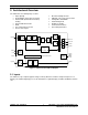
FS453/4 AND FS455/6 DATA SHEET: HARDWARE REFERENCE 2. Architectural Overview The FS453 has the following major sections: Color Space Conv.
FS453/4 AND FS455/6 DATA SHEET: HARDWARE REFERENCE 2.1.1 Input to Output Conversion Matrix Table 1 below lists some commonly used input modes and the correspondingly supported output modes. SDTV input dimensions are completely configurable, subject only to pixel clock range limitations. Input Configuration Output Configuration SDTV Pixels Lines HDTV NTSC PAL 480p 720p 1080i @59.
FS453/4 AND FS455/6 DATA SHEET: HARDWARE REFERENCE 2.4 Patented 2D Flicker Filter The Patented 2D Flicker Filter receives video lines from the 2D Scaler and performs vertical filtering to reduce or eliminate perceived flicker that is an artifact of the interlaced television format. The FS453's flicker filter is significantly more effective than a typical three-line-average flicker filter. The FS453’s flicker filter consists of joint horizontal (Sharpness) and vertical (Flicker) controls.
FS453/4 AND FS455/6 DATA SHEET: HARDWARE REFERENCE is used to achieve the finest clock resolution, using a dithered clock. In PLL mode, the NCO is bypassed and the clock is not dithered. The NCO can be used when HTOTAL and VTOTAL values have additional constraints that prevent selection of values that are factors of the TV pixel rate. 2.12 Serial Control Interface The FS453 registers are accessed through a serial input/output bus (SIO) which is I2C*-compatible and SMBus-compatible.
FS453/4 AND FS455/6 DATA SHEET: HARDWARE REFERENCE 3. Technical Highlights Creating clear, broadcast quality television video from high resolution computer graphics is a complex process. PC-to-TV Video Scan Converters have to surmount many technical obstacles. The most challenging of these are scaling, flicker reduction, and encoding. 3.
FS453/4 AND FS455/6 DATA SHEET: HARDWARE REFERENCE 3.2 Flicker Reduction Computer images are displayed progressively. That is, for a given frame of video, each line of video is scanned onto the monitor sequentially. SDTV images, however, are interlaced. Each SDTV frame of video is broken into two fields (one composed of odd lines and the other of even lines). First the odd lines are scanned onto the TV, and then the even lines are scanned onto the TV.
FS453/4 AND FS455/6 DATA SHEET: HARDWARE REFERENCE 3.3 Video Encoding Unlike component video formats (PC and HDTV) that process the color information separately to avoid interference, broadcast SDTV combines all picture information into a single, composite signal.
FS453/4 AND FS455/6 DATA SHEET: HARDWARE REFERENCE 4. Scaling and Positioning Notes The FS453 graphics converter does not use a frame memory. Therefore, the FS453 input video frame rate must be synchronous to and match the output video field or frame rate. In SDTV modes, the FS453 uses internal line memories in order to perform horizontal and vertical scaling. This imposes certain requirements on the scale and position settings. 4.
FS453/4 AND FS455/6 DATA SHEET: HARDWARE REFERENCE 4.2 Horizontal Scaling While vertical scaling is linked to the VTOTAL ratio, horizontal scaling is arbitrary and not linked to HTOTAL at all. The horizontal scaler is simply programmed with the ratio desired between TV_HACTIVE and GCC_HACTIVE. (See Figure 6 below.) Like vertical scaling, TV_HACTIVE is the desired number of pixels the image should occupy, not necessarily the number of active pixels for the selected TV standard.
FS453/4 AND FS455/6 DATA SHEET: HARDWARE REFERENCE 5. Pin Assignments Figure 7: PQFP Pin Diagram Pin 1. 2. 3. 4. 5. 6. 7. 8. 9. 10. 11. 12. 13. 14. 15. 16. 17. 18. 19. 20. Name VDD_DAD GPIO3 GPIO2 VSS_18 P0 P1 P2 P3 P4 P5 P6 P7 P8 P9 P10 P11 P12/V656_0 P13/V656_1 VDD_33 VDD_18 Pin 21. 22. 23. 24. 25. 26. 27. 28. 29. 30. 31. 32. 33. 34. 35. 36. 37. 38. 39. 40.
JANUARY, 2005, VERSION 3.
FS453/4 AND FS455/6 DATA SHEET: HARDWARE REFERENCE 5.1 FS453 ⇔ GCC Pin Mapping Table 3 below maps the FS453 pins to the host GCC controller chip.
FS453/4 AND FS455/6 DATA SHEET: HARDWARE REFERENCE 5.2 Pin Descriptions Pin Name FBGA Pin Number PQFP Pin Number Type/Value Pin Function Description Clocks CLKOUT D13 56 GTL/LVCMOS output CLKIN_P E13 54 Differential input CLKIN_N G12 51 Differential input XTAL_IN B10 63 LVTTL input XTAL_OUT A11 62 LVTTL output Pixel Clock Output. Clock to Graphics Control Chip (GCC) clock input. Synthesized from XTAL_IN. 0.78125 to 150 MHz range. Supports 1.5 to 3.3 volt CMOS or GTL.
FS453/4 AND FS455/6 Pin Name DATA SHEET: HARDWARE REFERENCE BLANK FBGA Pin Number M11 PQFP Pin Number 38 FIELD N10 37 JANUARY, 2005, VERSION 3.0 Type/Value Pin Function Description GTL/TTL input Digital BLANK VGA input. True outside of GCC active area. Connects to GCC blank pin (or to ground if a GCC blank pin is not available). GTL/TTL Digital FIELD output. Delay and polarity output programmable. 18 COPYRIGHT ©2003-4 FOCUS ENHANCEMENTS, INC.
FS453/4 AND FS455/6 Pin Name DATA SHEET: HARDWARE REFERENCE FBGA Pin Number PQFP Pin Number Video Outputs DAC_A A8 68 analog video DAC_B A7 70 analog video DAC_C A6 72 analog video DAC_D A9 66 analog video Voltage Reference RSVD1 Type/Value 76 Video output. As programmed by the DAC_CNTL (9Eh) register. Video output. As programmed by the DAC_CNTL (9Eh) register. Video output. As programmed by the DAC_CNTL (9Eh) register. Video output. As programmed by the DAC_CNTL (9Eh) register.
FS453/4 AND FS455/6 DATA SHEET: HARDWARE REFERENCE Pin Name FBGA Pin Number Power and Ground VDD_PA C12 PQFP Pin Number Type/Value Pin Function Description 59 +3.3 V B11 61 +3.3 V VDD_33 J13,L2,M 7 19,30,46 +3.3 V VDD_O D12 57 VDD_18 B13,J12, M1,N13 B2 20,40,47, 60 1 B5,B6,B7, B8 C13 67,69,71, 73 58 0V D/A Converter Power. Filtered 3.3 volt power for 10 bit video D/A converters. CLKOUT phase-locked loop Ground. A10 64 0V TV Crystal Oscillator Ground.
FS453/4 AND FS455/6 DATA SHEET: HARDWARE REFERENCE 6. Control Register Function Map Table 5 below lists the Control Register functions and register numbers. For more information about the Control Registers, please consult the FS453/4 and FS455/6 Software / Firmware Reference. 6.1 Register Reference Table The General Function labels of the FS453 registers are intended to help design engineers determine which registers will affect specific functions of the FS453.
FS453/4 AND FS455/6 DATA SHEET: HARDWARE REFERENCE General Function SDTV Output Name Offset Default Value MISC_47 47h 00h SDTV Output HSYNC_WID 48h 7Eh SDTV Output BURST_WID 49h 44h SDTV Output BPORCH 4Ah 76h SDTV Output CB_BURST 4Bh 3Bh SDTV Output CR_BURST 4Ch 00h SDTV Output MISC_4D 4Dh 00h SDTV Output BLACK_LVL 4Eh 0246h SDTV Output BLANK_LVL 50h 003Ch SDTV Output NUM_LINES 57h 0183h SDTV Output WHITE_LVL 5Eh 00C8h SDTV Output CB_GAIN 60h 89h SDTV Out
FS453/4 AND FS455/6 DATA SHEET: HARDWARE REFERENCE General Function Color Matrix Name Offset Default Value RED_MTX A2h 0000h Color Matrix GRN_MTX A4h 0000h Color Matrix BLU_MTX A6h 0000h Color Matrix RED_SCL A8h 0000h Color Matrix GRN_SCL AAh 0000h Color Matrix BLU_SCL ACh 0000h SDTV Output CLOSED CAPTION FIELD 1 AEh 0000h SDTV Output CLOSED CAPTION FIELD 2 B0h 0000h SDTV Output B2h 0000h B4h 0000h B6h 0000h HDTV Output CLOSED CAPTION CONTROL CLOSED CAPTION BLANK
FS453/4 AND FS455/6 DATA SHEET: HARDWARE REFERENCE 7. Specifications 7.1 Absolute Maximum and Recommended Ratings (Beyond which the device may be damaged)(a) Parameter Power Supply Voltages VDD-33 (Measured to VSS_33) VDD-18 (Measured to VSS_18) VDD-DAD (Measured to VSS_DAD) VDD-PA (Measured to VSS_PA) VDD-DA (Measured to VSS_DA) VDD-O (Measured to VSS_O) VDD-OSC (Measured to VSS_OSC) VSS-DA, VSS-DAD, VSS-PA, VSS-33, VSS-18, VSS-O, VSS-OSC (delta) Digital Inputs 3.
FS453/4 AND FS455/6 DATA SHEET: HARDWARE REFERENCE 7.2 Electrical Characteristics Parameter Power Supply Currents IDD-18 1.8 volt Digital current IDD-DA 3.3 volt DAC current IDD-DA 3.3 volt DAC current Conditions Min Core clk =50MHz RL=37.5Ω x 4 RL=37.5Ω x 4, DAC Low Power On IDD-OSC 3.3 volt Crystal Oscillator current CL=72pF,18pF Xtal IDD-DPA 3.3 volt Pixel PLL current LVTTL Inputs and Outputs CI Input Capacitance CO Output Capacitance IIH Input Current, HIGH VDD-33 = 3.3 ± 0.3V, VIN = max.
FS453/4 AND FS455/6 DATA SHEET: HARDWARE REFERENCE Parameter Scalable LVTTL (1.5 to 3.3V) Outputs IOH (3.3V) Output Current, Logic HIGH IOL (3.3V) Output Current, Logic LOW VOH (3.3V) Output Voltage, HIGH VOL (3.3V) Output Voltage, LOW IOH (2.5V) Output Current, Logic HIGH IOL (2.5V) Output Current, Logic LOW VOH (2.5V) Output Voltage, HIGH VOL (2.5V) Output Voltage, LOW IOH (1.8V) Output Current, Logic HIGH IOL (1.8V) Output Current, Logic LOW VOH (1.8V) Output Voltage, HIGH VOL (1.
FS453/4 AND FS455/6 DATA SHEET: HARDWARE REFERENCE 7.
FS453/4 AND FS455/6 DATA SHEET: HARDWARE REFERENCE 8. Mechanical Dimensions 8.1 80-Lead PQFP Package Symbol A A1 A2 D D1 E E1 e L b α ddd ccc Tols. \ Leads MAX. +.10 / -.05 +/- .25 +/- .10 +/- .25 +/- .10 BASIC + .15 / -.10 +/- .05 MAX. Millimeters 2.35 0.25 MAX. 2.00 17.20 14.00 17.20 14.00 .65 .88 .30 0º – 7º .12 NOM. .10 Notes: 1. All dimensions in millimeters. 2. Dimensions shown are nominal with tolerances as indicated. 3. Foot length "L" is measured at gage plane, 0.25 above seating plane.
FS453/4 AND FS455/6 DATA SHEET: HARDWARE REFERENCE 8.2 88-Lead FBGA Package Figure 10 FBGA Package Outline & Dimensions JANUARY, 2005, VERSION 3.0 29 COPYRIGHT ©2003-4 FOCUS ENHANCEMENTS, INC.
FS453/4 AND FS455/6 DATA SHEET: HARDWARE REFERENCE 9. Component Placement This section gives guidelines for the placement and layout of components associated with the FS453. A printed circuit board (PCB) with a minimum of four layers is recommended for all designs utilizing the FS453. We recommend that layers 1 (top) and 4 (bottom) are used for signals, and that layers 2 and 3 are used for power and ground respectively.
FS453/4 AND FS455/6 DATA SHEET: HARDWARE REFERENCE Figure 11: Recommended Power Filter Networks 9.1.2 Ground Connect the analog and digital grounds of the FS453 to separate ground planes. This will insure that electrical noise from the digital ground does not pollute the analog ground. Connect these two planes with either a ferrite bead or a very thin trace. This will allow the two planes to maintain an equal voltage potential.
FS453/4 AND FS455/6 DATA SHEET: HARDWARE REFERENCE 9.2.2 Video Inputs The digital pixel data and the pixel clock of the FS453 may toggle at speeds up to 150 MHz (depending on input mode). It is critical that the traces used for these signals be kept as short as possible. They should be isolated from the analog outputs and analog circuitry. The signals carried on these traces are single ended high-speed signals and should be routed together as a bus.
FS453/4 AND FS455/6 DATA SHEET: HARDWARE REFERENCE 9.3.1.2 Suggested Output Filter Network Figure 12 below shows the suggested output filter network for the FS453. Note that SDTV and HDTV use different values. Figure 12: Recommended Output Filter JANUARY, 2005, VERSION 3.0 33 COPYRIGHT ©2003-4 FOCUS ENHANCEMENTS, INC.
FS453/4 AND FS455/6 DATA SHEET: HARDWARE REFERENCE The recommended network shown in Figure 12 on page 33 will deliver robust video quality. It incorporates a source-terminating 75 Ohm resistor and a filter tuned for 37.5 Ohm impedance (assuming a matching 75 Ohm terminating resistor at the load). Table 10 below shows the correct component values to use for typical Standard and High Definition Television applications.
FS453/4 AND FS455/6 DATA SHEET: HARDWARE REFERENCE graphics controller’s digital video data. The timing of the variable pixel clock is critical; any disturbances to this signal will translate directly into noise on the video output. The best method to stabilize the variable pixel clock signal is to source terminate the signal with a load that matches the impedance of the signal trace.
FS453/4 AND FS455/6 DATA SHEET: HARDWARE REFERENCE 9.4.3.1 Pseudo-master Mode In Pseudo-master Mode shown below, the FS453 has complete control of the graphics system clock, but relinquishes the video sync signals to the GCC. The GCC provides the FS453 with a complete complement of digital video signals at the rate of the FS453 clock (CLKOUT). PSEUDO-MASTER MODE DIAGRAM DATA GCC FS453 SYNC 27 CLK IN CLK OUT Figure 13: Pixel Clock Pseudo-master Mode 9.4.3.
FS453/4 AND FS455/6 DATA SHEET: HARDWARE REFERENCE 9.5 EMI Case Study The following notes are from an engineer's experiences passing a new board through EMI testing. 1) You may need to analyze your board trace characteristic impedance, and adjust the optimal termination. If you can slowdown the edges without disturbing your timing, you can exorcise the (unnecessary) higher harmonics that can scoot across close trace clearances as if they were short circuits.
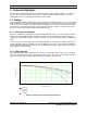
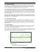
FS453/4 AND FS455/6 DATA SHEET: HARDWARE REFERENCE 9.6 Solder Re-flow Profiles The following figures provide solder re-flow profiles for the PQFP and FBGA packages with lead and lead-free solder options. IR ReRe-flow Profile °C 300 E (Peak Temperature 235°C +5, -0 °C) C 200 D 100 F B A sec IR Re-flow Profile for Pre-conditioning Peak Temp. Max. 240°C Heat-up(A) Pre-heat(B) 3°C/sec Max. 140~160°C 60~120sec Heat-up(C) Maintain(D) Re-flow peak(E) Cooling down(F) 3°C/sec Max.
FS453/4 AND FS455/6 DATA SHEET: HARDWARE REFERENCE IR ReRe-flow Profile °C 300 E (Peak Temperature 220°C +5, -0 °C) C 200 F D 100 B A sec IR Re-flow Profile for Pre-conditioning Peak Temp. Max. 225°C Heat-up(A) Pre-heat(B) 3°C/sec Max. 140~160°C 60~120sec Heat-up(C) Maintain(D) Re-flow peak(E) Cooling down(F) 3°C/sec Max. 60~150sec (Over 183°C) Max. 220 +5, -0 °C 10sec ±3sec 6°C/sec max.
FS453/4 AND FS455/6 DATA SHEET: HARDWARE REFERENCE 10. Revision History August 30, 2002: Release V1.1. Data Sheet reorganized into separate reference guides. The new Data Sheet package consists of a Product Brief, Hardware Reference, Software/Firmware Reference, and a Physical (Layout) Reference. January 13, 2003: Release V2.0. Expanded Introduction and Architectural Overview. Added new sections: Technical Highlights and Scaling and Positioning Notes.
FS453/4 AND FS455/6 DATA SHEET: HARDWARE REFERENCE 11.