
User's Manual

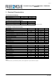
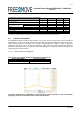
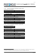
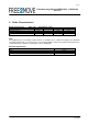
Table Of Contents
- 1 Device pinout
- 2 Device terminal functions
- 3 Electrical Characteristics
- 4 Radio Characteristics
- Firmware versions
- 5 Device terminal description
- 6 Application information
- 7 Package information
- 8 Certifications
- 9 RoHS And REACH Statement
- 10 Tape and Reel information
- 11 Ordering information
- 12 Document history
- Acronyms and definitions

Rev: e
© 2030 Free2move AB
Page 6(45)
Extended range Bluetooth
Module - F2M03GXA
Datasheet
Input/Output Terminal Characteristics (Continued)
Auxiliary ADC, 8
-
bit resolution
Min
Typ
Max
Unit
Resolution
- - 8 Bits
Input voltage range
(LSB size = 1.8/255= 7.1mV)
0 - 1.8 V
Accuracy
(Guaranteed monotonic)
INL -1 - 1 LSB
DNL 0 - 1 LSB
Offset -1 - 1 LSB
Gain Error -0.8 - 0.8 %
Input Bandwidth - 100 - KHz
Conversion time - 2.5 - µS
Sample rate*
- - 700 Sample/s
*The ADC is accessed through the VM function. The sample rate given is achieved as a part of this function
3.1 Current consumption
The F2MGXA module is power by dual voltages, one for logic and I/O, and the other for the FEM (Front
End Module, LNA / PA). These two voltages are connected separately externally but can be driven by one
single voltage regulator. Preferably, two separate voltage regulators should be used to minimize
interference from logic and I/O on the radio frequency signal. Due to the nature of Bluetooth, switching
between transmit and receive, the regulator must be able manage fast changes in current consumption, not
adding extensive amount of noise.
3.1.1 Peek current consumption
Peek current consumption during TX with different output powers
Outp
ut power [dBm]
Peek current [mA]
0 162
18 242
The Figure show when the F2M03GXA receive and transmit a packet acting as a slave in sniff mode
(duty cycle of 200 ms). The peek current is 232 mA in this figure.