
Datasheet


2
Data Sheet
512 Kbit / 1 Mbit / 2 Mbit Many-Time Programmable Flash
GLS27SF512 / GLS27SF010 / GLS27SF020
©2010 Greenliant Systems, Ltd. S71152-13-000 05/10
have been stable for at least T
CE
-T
OE.
When the CE# pin is
high, the chip is deselected and a typical standby current of
10 µA is consumed. OE# is the output control and is used
to gate data from the output pins. The data bus is in high
impedance state when either CE# or OE# is high.
Byte-Program Operation
The GLS27SF512/010/020 are programmed by using an
external programmer. The programming mode for
GLS27SF010/020 is activated by asserting 11.4-12V on
V
PP
pin, V
DD
= 4.5-5.5V, V
IL
on CE# pin, and V
IH
on OE#
pin. The programming mode for GLS27SF512 is activated
by asserting 11.4-12V on OE#/V
PP
pin, V
DD
= 4.5-5.5V,
and V
IL
on CE# pin. These devices are programmed byte-
by-byte with the desired data at the desired address using
a single pulse (CE# pin low for GLS27SF512 and PGM#
pin low for GLS27SF010/020) of 20 µs. Using the MTP
programming algorithm, the Byte-Programming process
continues byte-by-byte until the entire chip has been pro-
grammed.
Chip-Erase Operation
The only way to change a data from a “0” to “1” is by electri-
cal erase that changes every bit in the device to “1”. Unlike
traditional EPROMs, which use UV light to do the Chip-
Erase, the GLS27SF512/010/020 uses an electrical Chip-
Erase operation. This saves a significant amount of time
(about 30 minutes for each Erase operation). The entire
chip can be erased in a single pulse of 100 ms (CE# pin
low for GLS27SF512 and PGM# pin for GLS27SF010/
020). In order to activate the Erase mode for
GLS27SF010/020, the 11.4-12V is applied to V
PP
and A
9
pins, V
DD
= 4.5-5.5V, V
IL
on CE# pin, and V
IH
on OE# pin.
In order to activate Erase mode for GLS27SF512, the 11.4-
12V is applied to OE#/V
PP
and A
9
pins, V
DD
= 4.5-5.5V,
and V
IL
on CE# pin. All other address and data pins are
“don’t care”. The falling edge of CE# (PGM# for
GLS27SF010/020) will start the Chip-Erase operation.
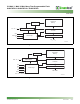
Once the chip has been erased, all bytes must be verified
for FFH. Refer to Figures 13 and 14 for the flowcharts.
Product Identification Mode
The Product Identification mode identifies the devices as
the GLS27SF512, GLS27SF010 and GLS27SF020 and
manufacturer as Greenliant. This mode may be accessed
by the hardware method. To activate this mode for
GLS27SF010/020, the programming equipment must force
V
H
(11.4-12V) on address A
9
with V
PP
pin at V
DD
(4.5-5.5V)
or V
SS
. To activate this mode for GLS27SF512, the pro-
gramming equipment must force V
H
(11.4-12V) on address
A
9
with OE#/V
PP
pin at V
IL
. Two identifier bytes may then
be sequenced from the device outputs by toggling address
line A
0
. For details, see Tables 3 and 4 for hardware opera-
tion.
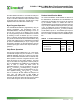
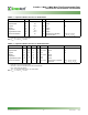
TABLE 1: Product Identification
Address Data
Manufacturer’s ID 0000H BFH
Device ID
GLS27SF512 0001H A4H
GLS27SF010 0001H A5H
GLS27SF020 0001H A6H
T1.2 1152