
Datasheet


Data Sheet
512 Kbit / 1 Mbit / 2 Mbit Many-Time Programmable Flash
GLS27SF512 / GLS27SF010 / GLS27SF020
5
©2010 Greenliant Systems, Ltd. S71152-13-000 05/10
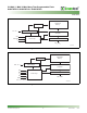
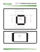
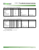
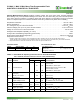
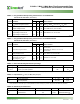
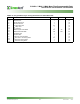
FIGURE 5: Pin Assignments for 28-pin and 32-pin PDIP
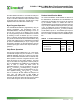
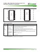
TABLE 2: Pin Description
Symbol Pin Name Functions
A
MS
1
-A
0
1. A
MS
= Most significant address
A
MS
= A
15
for GLS27SF512, A
16
for GLS27SF010, and A
17
for GLS27SF020
Address Inputs To provide memory addresses
DQ
7
-DQ
0
Data Input/output To output data during Read cycles and receive input data during Program cycles
The outputs are in tri-state when OE# or CE# is high.
CE# Chip Enable To activate the device when CE# is low
OE# Output Enable For GLS27SF010/020, to gate the data output buffers during Read operation
OE#/V
PP
Output Enable/V
PP
For GLS27SF512, to gate the data output buffers during Read operation and high voltage
pin during Chip-Erase and programming operation
V
PP
Power Supply for
Program or Erase
For GLS27SF010/020, high voltage pin during Chip-Erase and programming operation
11.4-12V
V
DD
Power Supply To provide 5.0V supply (4.5-5.5V)
V
SS
Ground
NC No Connection Unconnected pins.
T2.4 1152
1
2
3
4
5
6
7
8
9
10
11
12
13
14
15
16
32-pin
PDIP
To p Vi e w
V
PP
A16
A15
A12
A7
A6
A5
A4
A3
A2
A1
A0
DQ0
DQ1
DQ2
V
SS
V
PP
A16
A15
A12
A7
A6
A5
A4
A3
A2
A1
A0
DQ0
DQ1
DQ2
V
SS
32
31
30
29
28
27
26
25
24
23
22
21
20
19
18
17
V
DD
PGM#
NC
A14
A13
A8
A9
A11
OE#
A10
CE#
DQ7
DQ6
DQ5
DQ4
DQ3
V
DD
PGM#
A17
A14
A13
A8
A9
A11
OE#
A10
CE#
DQ7
DQ6
DQ5
DQ4
DQ3
1152 32-pdip P4.2
GLS27SF010 GLS27SF010GLS27SF020 GLS27SF020
1
2
3
4
5
6
7
8
9
10
11
12
13
14
28-pin
PDIP
To p Vi e w
A15
A12
A7
A6
A5
A4
A3
A2
A1
A0
DQ0
DQ1
DQ2
V
SS
28
27
26
25
24
23
22
21
20
19
18
17
16
15
V
DD
A14
A13
A8
A9
A11
OE#/ V
PP
A10
CE#
DQ7
DQ6
DQ5
DQ4
DQ3
1152 28-pdip P3.2
GLS27SF512GLS27SF512