
Datasheet


Data Sheet
512 Kbit / 1 Mbit / 2 Mbit Many-Time Programmable Flash
GLS27SF512 / GLS27SF010 / GLS27SF020
7
©2010 Greenliant Systems, Ltd. S71152-13-000 05/10
Absolute Maximum Stress Ratings (Applied conditions greater than those listed under “Absolute Maximum
Stress Ratings” may cause permanent damage to the device. This is a stress rating only and functional operation
of the device at these conditions or conditions greater than those defined in the operational sections of this data
sheet is not implied. Exposure to absolute maximum stress rating conditions may affect device reliability.)
Temperature Under Bias . . . . . . . . . . . . . . . . . . . . . . . . . . . . . . . . . . . . . . . . . . . . . . . . . . . . . . . . . -55°C to +125°C
Storage Temperature . . . . . . . . . . . . . . . . . . . . . . . . . . . . . . . . . . . . . . . . . . . . . . . . . . . . . . . . . . . -65°C to +150°C
D. C. Voltage on Any Pin to Ground Potential . . . . . . . . . . . . . . . . . . . . . . . . . . . . . . . . . . . . . . . . -0.5V to V
DD
+0.5V
Transient Voltage (<20 ns) on Any Pin to Ground Potential . . . . . . . . . . . . . . . . . . . . . . . . . . . . . -2.0V to V
DD
+2.0V
Voltage on A
9
and V
PP
Pin to Ground Potential . . . . . . . . . . . . . . . . . . . . . . . . . . . . . . . . . . . . . . . . . -0.5V to 14.0V
Package Power Dissipation Capability (T
A
= 25°C) . . . . . . . . . . . . . . . . . . . . . . . . . . . . . . . . . . . . . . . . . . . . . 1.0W
Through Hole Lead Soldering Temperature (10 Seconds) . . . . . . . . . . . . . . . . . . . . . . . . . . . . . . . . . . . . . . . 300°C
Surface Mount Solder Reflow Temperature
1
. . . . . . . . . . . . . . . . . . . . . . . . . . . . . . . . . . . . . . 260°C for 10 seconds
Output Short Circuit Current
2
. . . . . . . . . . . . . . . . . . . . . . . . . . . . . . . . . . . . . . . . . . . . . . . . . . . . . . . . . . . . 100 mA
1. Excluding certain with-Pb 32-PLCC units, all packages are 260°C capable in both non-Pb and with-Pb solder versions.
Certain with-Pb 32-PLCC package types are capable of 240
°C for 10 seconds; please consult the factory for the latest information.
2. Outputs shorted for no more than one second. No more than one output shorted at a time.
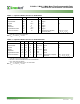
OPERATING RANGE
Range Ambient Temp V
DD
V
PP
Commercial 0°C to +70°C 4.5-5.5V 11.4-12V
AC CONDITIONS OF TEST
Input Rise/Fall Time . . . . . . . . . . . 10 ns
Output Load . . . . . . . . . . . . . . . . . C
L
= 30 pF for 70 ns
See Figures 11 and 12
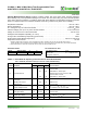
TABLE 5: Read Mode DC Operating Characteristics for GLS27SF512/010/020
V
DD
= 4.5-5.5V, V
PP
=V
DD
or V
SS
(T
A
= 0°C to +70°C (Commercial))
Symbol Parameter
Limits
Test ConditionsMin Max Units
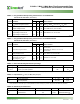
I
DD
V
DD
Read Current Address input=V
ILT
/V
IHT
at f=1/T
RC
Min
V
DD
=V
DD
Max
30 mA CE#=OE#=V
IL
, all I/Os open
I
PPR
V
PP
Read Current Address input=V
ILT
/V
IHT
at f=1/T
RC
Min
V
DD
=V
DD
Max, V
PP
=V
DD
100 µA CE#=OE#=V
IL
, all I/Os open
I
SB1
Standby V
DD
Current
(TTL input)
3mACE#=V
IH
, V
DD
=V
DD
Max
I
SB2
Standby V
DD
Current
(CMOS input)
100 µA CE#=V
DD
-0.3
V
DD
=V
DD
Max
I
LI
Input Leakage Current 1 µA V
IN
=GND to V
DD
, V
DD
=V
DD
Max
I
LO
Output Leakage Current 10 µA V
OUT
=GND to V
DD
, V
DD
=V
DD
Max
V
IL
Input Low Voltage 0.8 V V
DD
=V
DD
Min
V
IH
Input High Voltage 2.0 V
DD
+0.5 V V
DD
=V
DD
Max
V
OL
Output Low Voltage 0.2 V I
OL
=2.1 mA, V
DD
=V
DD
Min
V
OH
Output High Voltage 2.4 V I
OH
=-400 µA, V
DD
=V
DD
Min
I
H
Supervoltage Current for A
9
200 µA CE#=OE#=V
IL
, A
9
=V
H
Max
T5.6 1152