
Datasheet


Data Sheet
512 Kbit / 1 Mbit / 2 Mbit Many-Time Programmable Flash
GLS27SF512 / GLS27SF010 / GLS27SF020
9
©2010 Greenliant Systems, Ltd. S71152-13-000 05/10
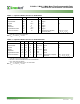
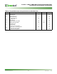
AC CHARACTERISTICS
TABLE 11: Read Cycle Timing Parameters V
DD
= 4.5-5.5V (T
A
= 0°C to +70°C (Commercial))
Symbol Parameter Min Max Units
T
RC
Read Cycle Time 70 ns
T
CE
Chip Enable Access Time 70 ns
T
AA
Address Access Time 70 ns
T
OE
Output Enable Access Time 35 ns
T
CLZ
1
1. This parameter is measured only for initial qualification and after a design or process change that could affect this parameter.
CE# Low to Active Output 0 ns
T
OLZ
1
OE# Low to Active Output 0 ns
T
CHZ
1
CE# High to High-Z Output 25 ns
T
OHZ
1
OE# High to High-Z Output 25 ns
T
OH
1
Output Hold from Address Change 0 ns
T11.3 1152
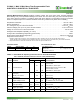
TABLE 12: Program/Erase Cycle Timing Parameters for GLS27SF512
Symbol Parameter Min Max Units
T
AS
Address Setup Time 1 µs
T
AH
Address Hold Time 1 µs
T
PRT
OE#/V
PP
Pulse Rise Time 50 ns
T
VPS
OE#/V
PP
Setup Time 1 µs
T
VPH
OE#/V
PP
Hold Time 1 µs
T
PW
CE# Program Pulse Width 20 30 µs
T
EW
CE# Erase Pulse Width 100 500 ms
T
DS
Data Setup Time 1 µs
T
DH
Data Hold Time 1 µs
T
VR
OE#/V
PP
and A
9
Recovery Time 1 µs
T
ART
A
9
Rise Time to 12V during Erase 50 ns
T
A9S
A
9
Setup Time during Erase 1 µs
T
A9H
A
9
Hold Time during Erase 1 µs
T12.0 1152