IFX24401 Low Dropout Voltage Regulator IFX24401TEV50 IFX24401ELV50 Data Sheet Rev. 1.
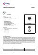
Low Dropout Voltage Regulator 1 IFX24401 Overview Features • • • • • • • • • • • Output voltage 5 V ±2% Ultra low current consumption: 20 µA (typ.) 300 mA current capability Enable input Very low-drop voltage Short circuit protection Overtemperature protection Low Dropout Voltage, 250mV (typ.) High Input Voltage 45 V Temperature Range -40 °C ≤ Tj ≤ 125 °C Green Product (RoHS compliant) PG-TO252-5 Applications • • • • • Battery powered devices (e.g.
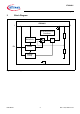
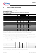
IFX24401 Block Diagram 2 Block Diagram IFX24401 I Q Overtemperature Shutdown Bandgap Reference EN 1 Enable Charge Pump GND Figure 1 Data Sheet Block Diagram 3 Rev. 1.
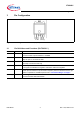
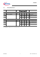
IFX24401 Pin Configuration 3 Pin Configuration I NC EN Q Figure 2 Pin Configuration PG-TO252-5 (top view) 3.1 Pin Definitions and Functions (PG-TO252-5 ) Pin Symbol Function 1 I Input Connect ceramic capcitor between I and GND 2 N.C. No Connect May be open or connected to GND 3 GND Ground Internally connected to heat slug 4 EN Enable Input Low signal level disables the regulator. Pull-down resistor is integrated. 5 Q Output Place capacitor between Q pin and GND.
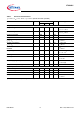
IFX24401 Pin Configuration 1 & 1 & 1 & , 1 & 1 & *1' 1 & 1 & 1 & (1 4 1 & 1 & 3,1&21),*B6623 69* Figure 3 Pin Configuration PG-SSOP-14 (top view) 3.2 Pin Definitions and Functions (PG-SSOP-14 ) Pin Symbol Function 1,2,3,5,7 N.C. No Connect May be open or connected to GND 4 GND Ground 6 EN Enable Input Low signal level disables the regulator. Pull-down resistor is integrated. 8,10,11,1 2,14 N.C.
IFX24401 General Product Characteristics 4 General Product Characteristics 4.1 Absolute Maximum Ratings Absolute Maximum Ratings1) Tj = -40 °C to 150 °C; all voltages with respect to ground, positive current flowing into pin (unless otherwise specified) Parameter Symbol Limit Values Min. Unit Test Condition Max. Input I Voltage Current VI II -0.3 45 V – -1 – mA – VEN -0.3 45 V Observe current limit IEN -1 1 mA – VQ VQ IQ -0.3 5.5 V – -0.3 6.
IFX24401 General Product Characteristics 4.3 Pos. Thermal Resistance Parameter Symbol Limit Value Min. Typ. Unit Conditions Max. IFX24401TEV50 (PG-TO252-5, ) 4.3.1 Junction to Case1) RthJC RthJA – 4 – K/W measured to pin 5 – 115 – K/W Footprint only2) 4.3.3 – 57 – K/W 300mm2 heatsink area on PCB2) 4.3.4 – 42 – K/W 600mm2 heatsink area on PCB2) – 7 – K/W measured to pin 5 – 120 – K/W Footprint only2) 4.3.7 – 59 – K/W 300mm2 heatsink area on PCB2) 4.3.
IFX24401 General Product Characteristics Table 1 Electrical Characteristics VI = 13.5 V; VEN = 5 V; -40 °C < Tj < 125 °C (unless otherwise specified) Parameter Symbol Limit Values Min. Typ. Max. Unit Measuring Condition Output Q Output voltage VQ 4.9 5.0 5.1 V 0.1 mA < IQ < 300 mA; 6 V < VI < 16 V Output voltage VQ 4.9 5.0 5.1 V 0.
IFX24401 Typical Performance Characteristics 5 Typical Performance Characteristics Current Consumption Iq versus Junction Temperature TJ Current Consumption Iq versus Input Voltage VQ 1_Iq -Tj .v s d 3_IQ -V I.V S D Iq [µA ] T J = 25 °C Iq [µA] VI = 13.5V 100 40 IQ = 100 µA 10 IQ = 50mA 30 IQ = 10mA 20 1 I Q = 0.2mA 10 0.
IFX24401 Typical Performance Characteristics Dropout Voltage Vdr versus Output Current IQ Maximum Output Current IQ versus Junction Temperature Tj 6_V DR-IQ .V S D 600 8_IQMA X -TJ . V S D 620 Vdr [mV ] VI = 13.5 V IQ [mA ] T J = 150 °C 400 580 TJj = 25 °C 300 560 200 540 TJ = -40 °C 100 520 0 100 200 500 -40 -20 300 0 20 40 60 80 100 120 140 IQ [mA] Dropout Voltage Vdr versus Junction Temperature TJ [°C] Maximum Output Current IQ versus Input Voltage VI 7_V DR-TJ .
IFX24401 Typical Performance Characteristics Output Voltage VQ Start-up behavior Region of Stability 14_V Itime _s tartup. v s d 12_ESR-IQ.VSD 100 CQ = 10nF ...10 µF Tj = 25 °C ESRCQ [Ω] VQ [V] EN = HIGH 10 5.05 1 IQ = 5mA 5.00 Stable Region 4.90 0.1 4.80 0.01 0 50 100 150 200 2 1 3 Power Supply Ripple Rejection PSRR versus Frequency f t [ms] Load Regulation ∆VQ versus Output Current Change ∆IQ 13_P S RR.
IFX24401 Typical Performance Characteristics Load Regulation ∆VQ versus Output Current Change dIQ Line Regulation ∆VQ versus Input Voltage Changed VI 18b_dV Q-dIQ_V i135V. vs d 0 V I = 13 .5V ∆VQ 19_dV Q-dV I__150C.
IFX24401 Typical Performance Characteristics Line Regulation ∆VQ versus Input Voltage Change VI Load Transient Response Peak Voltage ∆VQ 19_dV Q-dV I_-40C. v sd 0 20_Load Tranc ient v s time 125. vs d T J =40 °C ∆VQ IQ ∆IQ =100mA [mV ] IQ = 1mA T J = 125 °C V I = 13.
IFX24401 Typical Performance Characteristics Line Transient Response Peak Voltage ∆VQ I Enabled Input Current IEN versus Input Voltage VI , EN=Off 25_IINH v s V IN INH _off . v s d 21_Line Tranc ient vs time 125. vs d T J = 125 °C VI = 13.5 V VI ∆VI = 2 V IEN [µA ] 1.0 EN = L (i.e. IC OFF) T J = 150 °C T J = 25 °C 0.8 TJ = -40°C 0.6 VQ 0.4 VQ = 50 mV/DIV 0.
IFX24401 Application Information 6 Application Information V Bat IFX24401 100 nF Overtemperature Shutdown Bandgap Reference e. g. Ignition 2 EN V CC Q 5 1 I 470 nF + 4.7 µF 1 Enable Charge Pump GND 3, Tab Figure 4 Application Diagram Input, Output An input capacitor is necessary for damping line influences. A resistor of approx. 1 Ω in series with CI, can damp the LC of the input inductivity and the input capacitor. The IFX24401 requires a ceramic output capacitor of at least 470 nF.
IFX24401 Package Outlines 7 Package Outlines 6.5 +0.15 -0.05 A 1) 2.3 +0.05 -0.10 0.9 +0.20 -0.01 0...0.15 0.51 MIN. 0.8 ±0.15 0.15 MAX. per side 0.5 +0.08 -0.04 B (5) (4.24) 1 ±0.1 9.98 ±0.5 6.22 -0.2 5.7 MAX. 0.5 +0.08 -0.04 5 x 0.6 ±0.1 1.14 0.1 B 4.56 0.25 M A B GPT09527 1) Includes mold flashes on each side. All metal surfaces tin plated, except area of cut. Figure 5 PG-TO252-5 0.15 M C A-B D 14x 0.64 ±0.25 1 8 1 7 0.2 M D 8x Bottom View 3 ±0.2 A 14 6 ±0.
IFX24401 Revision History 8 Revision History Revision Date Changes 1.02 2009-12-10 Corrections to pin assignment 1.01 2009-10-19 Coverpage changed Overview page: Inserted reference statement to TLE/TLF series. 1.0 2009-04-28 Initial Release Data Sheet 17 Rev. 1.
Edition 2009-12-10 Published by Infineon Technologies AG 81726 Munich, Germany © 2009 Infineon Technologies AG All Rights Reserved. Legal Disclaimer The information given in this document shall in no event be regarded as a guarantee of conditions or characteristics.