
Datasheet


Data Sheet 6 Rev. 1.02, 2009-12-10
IFX24401
General Product Characteristics
4 General Product Characteristics
4.1 Absolute Maximum Ratings
Note: Stresses above the ones listed here may cause permanent damage to the device. Exposure to absolute
maximum rating conditions for extended periods may affect device reliability.
Note: Integrated protection functions are designed to prevent IC destruction under fault conditions described in the
data sheet. Fault conditions are considered as “outside” normal operating range. Protection functions are
not designed for continuous repetitive operation.
4.2 Functional Range
Note: In the operating range, the functions given in the circuit description are fulfilled.
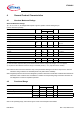
Absolute Maximum Ratings
1)
T
j
= -40 °C to 150 °C; all voltages with respect to ground, positive current flowing into pin
(unless otherwise specified)
1) Not subject to production test, specified by design.
Parameter Symbol Limit Values Unit Test Condition
Min. Max.
Input I
Voltage
V
I
-0.3 45 V –
Current
I
I
-1 – mA –
Enable EN
Voltage
V
EN
-0.3 45 V Observe current limit
I
EN,max
2)
2) External resistor required to keep current below absolute maximum rating when voltages ≥ 5.5 V are applied.
Current I
EN
-1 1 mA –
Output Q
Voltage
V
Q
-0.3 5.5 V –
Voltage
V
Q
-0.3 6.2 V t < 10 s
3)
3) Exposure to these absolute maximum ratings for extended periods (t > 10 s) may affect device reliability.
Current I
Q
-1 – mA –
Temperature
Junction temperature
T
j
-40 150 °C–
Storage temperature
T
stg
-50 150 °C–
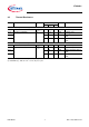
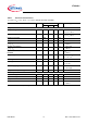
Parameter Symbol Limit Values Unit Remarks
Min. Max.
Input voltage
V
I
5.5 42 V –
Junction temperature
T
j
-40 125 °C–
Output Capacitor
C
Q
470 – nF
1)
1) The minimum output capacitance requirement is applicable for a worst case capacitor tolerance of 30%
ESR (C
Q
)– 10 Ω f = 10 kHz