IFX25001 Low Dropout Voltage Regulator Data Sheet Rev. 1.
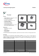
Low Dropout Voltage Regulator 1 IFX25001 Overview Features • • • • • • • • • • Output Voltages: 2.5, 3.3, 5.0, 8.5, or 10.
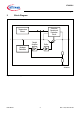
IFX25001 Block Diagram 2 Block Diagram Saturation Control and Protection Circuit Temperature Sensor Ι Q Control Amplifier Buffer Bandgap Reference GND AEB01959 Figure 1 Data Sheet Block Diagram 3 Rev. 1.
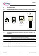
IFX25001 Pin Configuration 3 Pin Configuration 3.1 Pin Assignment PG-SOT223-4, PG-TO252-3, PG-TO263-3, and PG-TO220-3 *1' *1' *1' *1' , *1' 4 *1' , 627 6& YVG 4 3* 72 YVG , *1' 4 3* 72 YVG , *1' 4 3* 72 YVG Figure 2 Pin Configuration (top view) 3.2 Pin Definitions and Functions PG-SOT223-4, PG-TO252-3, PG-TO263-3, and PG-TO220-3 4 Pin No.
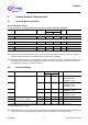
IFX25001 General Product Characteristics 4 General Product Characteristics 4.1 Absolute Maximum Ratings Absolute Maximum Ratings1) Tj = -40 °C to 150 °C; all voltages with respect to ground, (unless otherwise specified) Pos. Parameter Symbol Limit Values Min. Max. Unit Test Condition Input I 4.1.1 Voltage VI -42 45 V – Voltage VQ -1 40 V – Tj Tstg -40 150 °C – -50 150 °C – Output Q 4.1.2 Temperature 4.1.3 Junction temperature 4.1.
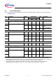
IFX25001 General Product Characteristics 4.3 Thermal Resistance Note: This thermal data was generated in accordance with JEDEC JESD51 standards. For more information, go to www.jedec.org. Pos. Parameter Symbol Limit Values Min. Typ. Max. Unit Conditions PG-TO252-3 4.3.1 Junction to Case1) RthJC – 4 – K/W measured to heat slug 4.3.2 Junction to Ambient1) – 27 – K/W 2) 4.3.3 RthJA RthJA – 57 – K/W 300 mm² heatsink area3) 4.3.
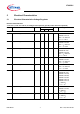
IFX25001 Electrical Characteristics 5 Electrical Characteristics 5.1 Electrical Characteristics Voltage Regulator Electrical Characteristics VI =13.5 V; Tj = -40 °C to 125 °C; all voltages with respect to ground (unless otherwise specified) Pos. Parameter Symbol Limit Values Min. Typ. Max. Unit Measuring Condition Output Q 5.1.1 Output Voltage VQ 9.6 10.0 10.4 V IFX25001 TS V10, IFX25001 TC V10 5 mA < IQ< 400 mA 11 V < VI < 28 V 5.1.1 Output Voltage VQ 8.16 8.5 8.
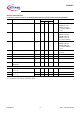
IFX25001 Electrical Characteristics Electrical Characteristics VI =13.5 V; Tj = -40 °C to 125 °C; all voltages with respect to ground (unless otherwise specified) Pos. Parameter Symbol Limit Values Min. Typ. Max. Unit Measuring Condition 5.1.7 Load Regulation ΔVQ, lo – 20 50 mV IFX25001 TS V50, IFX25001TF V50, IFX25001 TC V50, IQ = 5 mA to 400 mA VI = 6 V 5.1.8 Load Regulation ΔVQ, lo – 20 50 mV IFX25001 TS V85, IFX25001 TC V85 IFX25001 TS V10, IFX25001 TC V10 IQ = 5 mA to 400 mA 5.
IFX25001 Electrical Characteristics 5.
IFX25001 Electrical Characteristics 5.2.1 Typical Performance Characteristics Voltage Regulator (V50 Version) Output Voltage VQ versus Junction Temperature TJ Current Consumption Iq versus Input Voltage VI AED01966 5.2 AED02269 30 VQ V Ιq mA 5.1 20 VI = 13.5 V T j = 25 C R L = 20 Ω 5.0 10 4.9 4.8 -40 0 40 80 0 120 ˚C 160 0 10 20 30 Tj Output Voltage VQ versus Input Voltage VI Input Current II versus Input Voltage VI AED01968 6 VQ 50 V VΙ V VQ 5 AED01977 3.5 mA II 3.0 2.
IFX25001 Electrical Characteristics 5.2.2 Typical Performance Characteristics Voltage Regulator (V85 Version) Output Voltage VQ versus Junction Temperature TJ Current Consumption Iq versus Input Voltage VI AED01970 8.8 VQ AED02270 30 V Ιq 8.7 8.6 mA 20 VI = 13.5 V T j = 25 C R L = 20 Ω 8.5 10 8.4 8.3 8.2 -40 0 40 80 0 120 ˚C 160 0 10 20 30 Tj Output Voltage VQ versus Input Voltage VI Input Current II versus Input Voltage VI AED01972 12 VQ 50 V VΙ AED03051 3.5 mA II 3.
IFX25001 Electrical Characteristics 5.2.3 Typical Performance Characteristics Voltage Regulator (V10 Version) Output Voltage VQ versus Junction Temperature TJ Current Consumption Iq versus Input Voltage VI AED01974 10.3 AED02270 30 VQ V 10.2 Ιq 10.1 mA 20 VI = 13.5 V T j = 25 C R L = 20 Ω 10.0 9.9 10 9.8 9.
IFX25001 Electrical Characteristics 5.2.4 Typical Performance Characteristics Voltage Regulator (V33 and V25 Version) Output Voltage VQ versus Junction Temperature TJ (V33 Version) Output Voltage VQ versus Junction Temperature TJ (V25 Version) AED02288 3.5 AED02806 2.7 VQ VQ V V 2.6 3.4 VI = 6 V VI = 6 V 3.3 2.5 3.2 2.4 3.1 2.3 3.0 2.2 2.9 -40 0 40 80 2.
IFX25001 Electrical Characteristics 5.2.5 Typical Performance Characteristics Voltage Regulator (V33 and V25 Version) Current Consumption Iq versus Output Current IQ (Low Load) Current Consumption Iq versus Output Current IQ (High Load) AED02268 0.6 Iq mA Iq mA 0.5 50 T j = 25 ˚C VI = 13.5 V 0.4 40 0.3 30 0.2 20 0.1 10 0 0 10 20 30 AED02267 60 40 mA 0 60 T j = 25 ˚C VI = 13.
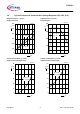
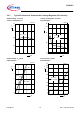
IFX25001 Package Outlines 6 Package Outlines 6.5 +0.15 -0.10 2.3 +0.05 -0.10 4.57 0.51 MIN. 0.15 MAX. per side 0.9 +0.08 -0.04 B 5.4 ±0.1 0.8 ±0.15 9.9 ±0.5 6.22 -0.2 1 ±0.1 A 3x 0.75 ±0.1 0...0.15 0.5 +0.08 -0.04 2.28 1 ±0.1 0.25 M A B 0.1 All metal surfaces tin plated, except area of cut. Figure 3 Data Sheet PG-TO252-3 15 Rev. 1.
IFX25001 Package Outlines 4.4 10 ±0.2 1.27 ±0.1 B 0.1 A 8.5 1) 0.05 2.4 2.7 ±0.3 4.7 ±0.5 7.55 1) 9.25 ±0.2 (15) 1 ±0.3 0...0.3 0...0.15 0.75 ±0.1 0.5 ±0.1 1.05 8˚ MAX. 2.54 5.08 0.25 M A B 1) Typical All metal surfaces: tin plated, except area of cut. Metal surface min. x=7.25, y=6.9 Figure 4 Data Sheet 0.1 B GPT09362 PG-TO263-3 16 Rev. 1.
IFX25001 Package Outlines 10 ±0.2 A 9.9 ±0.2 B 1) 2.8 ±0.2 4.4 1.27±0.1 0.05 C 0...0.15 13.5 ±0.5 4.55 ±0.2 2.4 9.25 ±0.2 1) 0...0.3 12.95 15.65 ±0.3 17±0.3 8.5 3.7 -0.15 0.5 ±0.1 3x 0.75 ±0.1 2.4 1.05 2x 2.54 1) Figure 5 Data Sheet 0.25 M A B C Typical All metal surfaces tin plated, except area of cut. Metal surface min. x=7.25, y=12.3 PG-TO220-3 17 Rev. 1.
IFX25001 Package Outlines 1.6 ±0.1 6.5 ±0.2 0.1 MAX. 2 B 0.5 MIN. 1 +0.2 acc. to DIN 6784 3.5 ±0.2 4 7 ±0.3 3 ±0.1 15˚ MAX. A 3 0.28 ±0.04 2.3 0.7 ±0.1 4.6 0.25 Figure 6 M A 0.25 M B PG-SOT223-4 Green Product (RoHS compliant) To meet the world-wide customer requirements for environmentally friendly products and to be compliant with government regulations the device is available as a green product. Green products are RoHS-Compliant (i.
IFX25001 Revision History 7 Revision History Revision Date Changes 1.02 2009-05-20 Editorial change (fig. 2) 1.01 2009-10-02 Coverpage changed Overview page: Inserted reference statement to TLE/TLF series. 1.0 2009-04-28 Initial Release Data Sheet 19 Rev. 1.
Edition 2010-05-20 Published by Infineon Technologies AG 81726 Munich, Germany © 2010 Infineon Technologies AG All Rights Reserved. Legal Disclaimer The information given in this document shall in no event be regarded as a guarantee of conditions or characteristics.