
Datasheet

IFX25001
General Product Characteristics
Data Sheet 5 Rev. 1.02, 2010-05-20
4 General Product Characteristics
4.1 Absolute Maximum Ratings
Note: Stresses above the ones listed here may cause permanent damage to the device. Exposure to absolute
maximum rating conditions for extended periods may affect device reliability.
Note: Integrated protection functions are designed to prevent IC destruction under fault conditions described in the
data sheet. Fault conditions are considered as “outside” normal operating range. Protection functions are
not designed for continuous repetitive operation.
4.2 Functional Range
Note: Within the functional or operating range, the IC operates as described in the circuit description. The electrical
characteristics are specified within the conditions given in the Electrical Characteristics table.
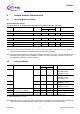
Absolute Maximum Ratings
1)
T
j
= -40 °C to 150 °C; all voltages with respect to ground, (unless otherwise specified)
1) not subject to production test, specified by design
Pos. Parameter Symbol Limit Values Unit Test Condition
Min. Max.
Input I
4.1.1 Voltage
V
I
-42 45 V –
Output Q
4.1.2 Voltage
V
Q
-1 40 V –
Temperature
4.1.3 Junction temperature
T
j
-40 150 °C–
4.1.4 Storage temperature
T
stg
-50 150 °C–
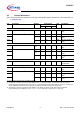
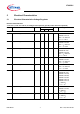
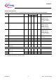
Pos. Parameter Symbol Limit Values Unit Remarks
Min. Max.
4.2.1 Input voltage
V
I
4.7 40 V IFX25001 ME V25
IFX25001 ME V33
IFX25001 TF V33
4.2.2
V
I
5.5 40 V IFX25001 TS V50
IFX25001TF V50
IFX25001 TC V50
4.2.3
V
I
9.0 40 V IFX25001 TS V85
IFX25001 TC V85
4.2.4
V
I
10.5 40 V IFX25001 TS V10
IFX25001 TC V10
4.2.5 Output Capacitor’s
Requirements for Stability
C
Q
22 – µF
1)
1) the minimum output capacitance requirement is applicable for a worst case capacitance tolerance of 30%
4.2.6 ESR(C
Q
) –3Ω
2)
2) relevant ESR value at f =10kHz
4.2.7 Junction temperature T
j
-40 125 °C–