
Datasheet

Data Sheet 6 Rev. 1.02, 2010-05-20
IFX25001
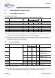
General Product Characteristics
4.3 Thermal Resistance
Note: This thermal data was generated in accordance with JEDEC JESD51 standards. For more information, go
to www.jedec.org.
Pos. Parameter Symbol Limit Values Unit Conditions
Min. Typ. Max.
PG-TO252-3
4.3.1 Junction to Case
1)
1) Not subject to production test, specified by design.
R
thJC
– 4 – K/W measured to heat
slug
4.3.2 Junction to Ambient
1)
R
thJA
–27–K/W
2)
2) Specified R
thJA
value is according to Jedec JESD51-2,-5,-7 at natural convection on FR4 2s2p board; The Product
(Chip+Package) was simulated on a 76.2 x 114.3 x 1.5 mm³ board with 2 inner copper layers (2 x 70µm Cu, 2 x 35µm Cu).
Where applicable a thermal via array under the exposed pad contacted the first inner copper layer.
4.3.3 R
thJA
– 57 – K/W 300 mm² heatsink
area
3)
3) Specified R
thJA
value is according to Jedec JESD 51-3 at natural convection on FR4 1s0p board; The Product
(Chip+Package) was simulated on a 76.2 × 114.3 × 1.5 mm
3
board with 1 copper layer (1 x 70µm Cu).
4.3.4 R
thJA
– 42 – K/W 600 mm² heatsink
area
3)
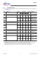
PG-TO263-3
4.3.5 Junction to Case
1)
R
thJC
– 4 – K/W measured to heat
slug
4.3.6 Junction to Ambient
1)
R
thJA
–22–K/W
2)
4.3.7 R
thJA
– 42 – K/W 300 mm² heatsink
area
3)
4.3.8 R
thJA
– 33 – K/W 600 mm² heatsink
area
3)
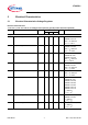
PG-TO220-3
4.3.9 Junction to Case
1)
R
thJC
– 8 – K/W measured to
exposed pad
PG-SOT223-4
4.3.10 Junction to Case
1)
R
thJC
– 25 – K/W measured to heat
slug
4.3.11 Junction to Ambient
1)
R
thJA
–51–K/W
2)
4.3.12 R
thJA
– 75 – K/W 300 mm² heatsink
area
3)
4.3.13 R
thJA
– 63 – K/W 600 mm² heatsink
area
3)